FP8 GEMM Optimization on AMD CDNA™4 Architecture#

This blog post continues our previous blog Matrix Core Programming on AMD CDNA™3 and CDNA™4 Architecture, which introduced Matrix Cores and demonstrated how to use them in HIP kernels.
In this post, we take the next step by showing how to use Matrix Cores in GEMM kernels, with a particular focus on optimizing an FP8 GEMM kernel on the AMD Instinct™ MI355X GPUs. If you are not yet familiar with Matrix Cores, we recommend reading the introductory post first and then returning to this article.
GPU Characteristics#
Compared with CDNA™3 architecture, the CDNA™4 architecture increases LDS capacity and read bandwidth (160 KB, 256 B/clk), expands the per-lane GLOBAL_LOAD_LDS transfer width (128-bit vs. 32-bit), and adds broader low-precision matrix-core support, including FP4/FP6 dense matrix fused-multiply-add (MFMA) and block-scaled MFMA instructions. Table 1 summarizes the architectural differences that matter most for this GEMM kernel design.
Feature |
CDNA™4 |
CDNA™3 |
|---|---|---|
Wavefront size |
|
|
LDS capacity |
|
|
LDS bank count |
|
|
LDS read bandwidth |
|
|
|
Up to |
Up to |
FP4/FP6 MFMA |
Supported |
Not supported |
Block-scaled MFMA |
Adds |
Not supported |
FP16/BF16 MFMA shapes |
Adds larger shapes ( |
Up to |
Table 1. Architectural differences between AMD CDNA™4 and CDNA™3 relevant to FP8 GEMM kernels.
Source data: AMD Instinct CDNA™4 ISA and AMD Instinct MI300 CDNA™3 ISA.
FP8 GEMM#
In this blog post, we will implement a GEMM kernel that computes \(C=A B^T\). The kernel multiplies matrix A of shape MxK with the transpose of matrix B which has shape NxK. The result is then written to matrix C of shape MxN. The input matrices are stored in row-major order and have FP8 (E4M3FN) data type. The output matrix has BF16 data type and is stored in row-major order as well. To minimize numerical accuracy loss during the computation, the accumulation is performed in FP32 precision.
To calculate the achieved FLOP/s, we use the following formula, given known kernel duration in seconds \(t\).
hipBLASLt Benchmark#
We use hipBLASLt as our performance target. The hipblaslt-bench script allows us to benchmark hipBLASLt FP8 GEMM for a specific matrix problem size using rotating buffers and warm-up iterations. For example, to benchmark hipBLASLt on matrix problem size M=N=K=4096:
hipblaslt-bench --api_method c --stride_a 0 --stride_b 0 --stride_c 0 --stride_d 0 \
  --alpha 1 --beta 0 --transA T --transB N --batch_count 1 --scaleA 1 --scaleB 1 \
  --a_type f8_r --b_type f8_r --c_type bf16_r --d_type bf16_r \
  --scale_type f32_r --bias_type f32_r --compute_type f32_r --rotating 512 \
  --iters 1000 --cold_iters 1000 -m 4096 -n 4096 -k 4096 \
  --lda 4096 --ldb 4096 --ldc 4096 --ldd 4096
Which gives ~2750 TFLOPS/s on the AMD MI355X. For M=N=K=8192, hipBLASLt achieves ~3130 TFLOPS/s[1]. Please refer to hipblaslt-bench for more information about the command line interface and available options.
Naive FP8 GEMM#
We start with the simplest version as a baseline. First, recall the GEMM form used here:
From this equation, the most direct mapping is: one thread computes one output element C[row, col]. That thread loops over k and accumulates the dot product. This is easy to implement, but it reloads A and B from global memory repeatedly, so it is expected to be memory-bound. The measured baseline result is 1.15 TFLOPS/s for M=N=K=4096.
Baseline code example:
__global__ void baseline_fp8_gemm_kernel(const fp8e4m3* A,
                                      const fp8e4m3* B,
                                      bf16* C,
                                      int M,
                                      int N,
                                      int K,
                                      int lda,
                                      int ldb,
                                      int ldc,
                                      float alpha,
                                      float beta) {
    const int row = blockIdx.y * blockDim.y + threadIdx.y;
    const int col = blockIdx.x * blockDim.x + threadIdx.x;
    if (row >= M || col >= N) {
        return;
    }

    // FP32 accumulation for one dot product.
    float acc = 0.0f;
    for (int k = 0; k < K; ++k) {
        acc += float(A[row * lda + k]) * float(B[col * ldb + k]);
    }
    const float c_prev = (beta == 0.0f) ? 0.0f : static_cast<float>(C[row * ldc + col]);
    //Write back in BF16.
    C[row * ldc + col] = bf16(alpha * acc + beta * c_prev);
}
LDS Tiling to Improve Data Reuse#
In the naive implementation, the main bottleneck is repeated global memory access and low arithmetic intensity. We address this with LDS tiling so that A and B data is reused across multiple output updates. This implementation improves performance from 1.15 TFLOPS/s to 4.80 TFLOPS/s for M=N=K=4096, but compute utilization is still low.
LDS-tiled code example:
__global__ void lds_tiled_fp8_gemm_kernel(const fp8e4m3* A,
                                      const fp8e4m3* B,
                                      bf16* C,
                                      int M,
                                      int N,
                                      int K,
                                      int lda,
                                      int ldb,
                                      int ldc,
                                      float alpha,
                                      float beta) {
    __shared__ float As[TILE_M][TILE_K];
    __shared__ float Bs[TILE_K][TILE_N];

    const int row = blockIdx.y * TILE_M + threadIdx.y;
    const int col = blockIdx.x * TILE_N + threadIdx.x;

    float acc = 0.0f;
    for (int k0 = 0; k0 < K; k0 += TILE_K) {
        As[threadIdx.y][threadIdx.x] = float(A[row * lda + (k0 + threadIdx.x)]);

        Bs[threadIdx.y][threadIdx.x] = float(B[col * ldb + (k0 + threadIdx.y)]);

        __syncthreads();

        for (int k = 0; k < TILE_K; ++k) {
            acc += As[threadIdx.y][k] * Bs[k][threadIdx.x];
        }

        __syncthreads();
    }

    const float c_prev = (beta == 0.0f) ? 0.0f : static_cast<float>(C[row * ldc + col]);
    C[row * ldc + col] = bf16(alpha * acc + beta * c_prev);
}
Matrix Core Instructions#
Currently, we don’t use any Matrix Core instructions and rely on slow FMA instructions for arithmetic operations. As a next step, we replace FMA with MFMA instructions. For the M=N=K=4096 case, this gives us a jump from 4.80 TFLOPS/s (LDS-tiled SIMT kernel) to 30.05 TFLOPS/s (MFMA matrix-core kernel) - ~6.3x performance increase.
On the CDNA™ architecture, MFMA is a wave-level matrix operation: all 64 lanes in a wave cooperate on D = A * B + C. That changes kernel design in two ways. First, operand layout is fixed by instruction semantics, so fragments must be staged in the expected lane mapping. Second, sustained performance depends on a balanced feed path: global memory -> LDS -> registers -> MFMA -> FP32 accumulator writeback.
The matrix-core variant used here is the 16x16x128 form with FP8 inputs and FP32 accumulation:
accumulator = matrix_core_op(input_a_fragment, input_b_fragment, accumulator);
To see what this change does in practice, Table 2 compares instruction issue rate (inst/cycle) and compute density (FLOPs/cycle) for the LDS-tiled SIMT path and the matrix-core path.
Kernel |
|
|
|
|
Total FLOPs/cycle |
|---|---|---|---|---|---|
LDS-tiled |
0 |
0.465838844 |
0 |
59.627372 |
59.627372 |
MFMA matrix-core kernel |
0.009418900 |
0.001177363 |
617.277051 |
0.150702 |
617.427753 |
Table 2. Instruction issue rate and compute density for the LDS-tiled `SIMT` kernel and the MFMA matrix-core kernel.
What this means in practice:
The LDS-tiled
SIMTkernel uses FMA, while the MFMA matrix-core kernel gets99.98%of its math from MFMA.The MFMA matrix-core kernel issues fewer math instructions per cycle than FMA, but each instruction is much heavier (
65536vs.128FLOPs/inst,512xlarger), so compute density rises sharply.Using
(inst/cycle) * (FLOPs/inst), the MFMA matrix-core kernel reaches about10.35xhigher FLOPs/cycle than the LDS-tiledSIMTkernel.
Figure 1 shows the lane and fragment layout used by the 16x16x128 matrix core instruction.
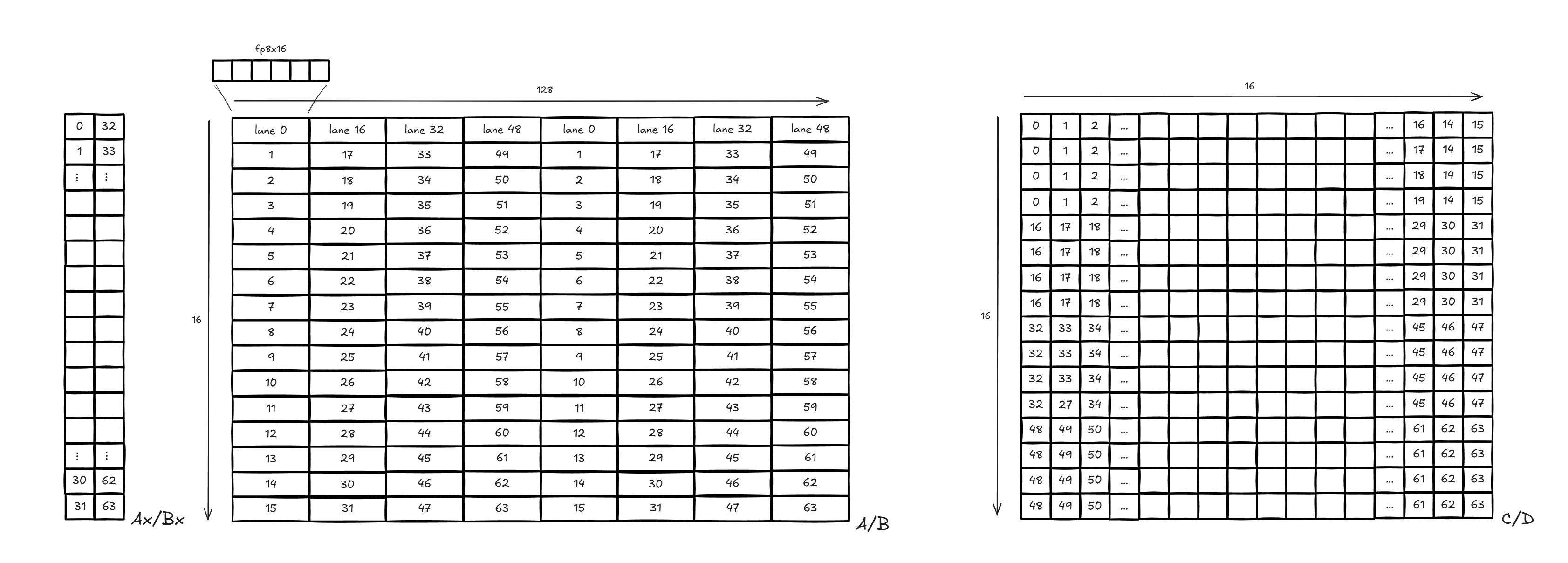
Figure 1: MFMA 16x16x128 Data Layout#
Wave-Lane Mapping in Practice#
Inside one wave (64 lanes), we split lane IDs into a row selector and a K-fragment selector:
const int lane = lane_in_wave;               // [0, 63]
const int row_in_tile = lane & 15;           // [0, 15]
const int row_group = lane >> 4;             // [0, 3], selects one 4-row output stripe

const int a_row = a_tile_row_start + row_in_tile;
const int b_row = b_tile_row_start + row_in_tile;   // B is arranged as [N, K]
const int k_chunk0 = row_group * 16;         // 0,16,32,48
const int k_chunk1 = k_chunk0 + 64;          // 64,80,96,112
For each K tile (128), one lane consumes:
A:32FP8 elements as two chunks (A_tile[a_row][k_chunk0 : k_chunk0+15]andA_tile[a_row][k_chunk1 : k_chunk1+15])B:32FP8 elements as two chunks (B_tile[b_row][k_chunk0 : k_chunk0+15]andB_tile[b_row][k_chunk1 : k_chunk1+15])
At writeback, each lane commits 4 FP32 accumulators (stored as BF16):
const int output_col = output_tile_col + row_in_tile;
const int output_row_start = output_tile_row + row_group * 4;

for (int t = 0; t < 4; ++t) {
    const int output_row = output_row_start + t;
    const float c_old = (beta == 0.0f) ? 0.0f : static_cast<float>(C[output_row * ldc + output_col]);
    C[output_row * ldc + output_col] = bf16(alpha * accum_fp32[t] + beta * c_old);
}
Vectorized Load#
The vectorized variant packs 16 FP8 values per load and writes directly to LDS.
This gives a clear step up from scalar loads by cutting instruction count and improving data ingress efficiency.
using fp8x16_t = __attribute__((vector_size(16))) fp8_t;

// Helper: load 16 FP8 values (16 bytes) from address p.
static inline __device__ fp8x16_t load_fp8x16_u4(const fp8_t* p) {
    const uint4 v = *reinterpret_cast<const uint4*>(p);
    return *reinterpret_cast<const fp8x16_t*>(&v);
}

const fp8x16_t a_vec = load_fp8x16_u4(A_storage + (base_m + r) * lda + (k0 + k));
*reinterpret_cast<fp8x16_t*>(&As[r][k]) = a_vec;

const fp8x16_t b_vec = load_fp8x16_u4(B_storage + (base_n + r) * ldb + (k0 + k));
*reinterpret_cast<fp8x16_t*>(&Bs[r][k]) = b_vec;
Compared with scalar FP8 loads, this reduces the per-lane load loop count for the same byte volume and improves ingress efficiency before matrix-core compute. Figure 2 makes that loop-count reduction visible for the same LDS payload, and from there the next step is to simplify global-to-LDS transfer even more.
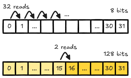
Figure 2: Read Count Comparison (Per Lane, Same LDS Payload)#
Direct Global-to-LDS Load#
At this step, we use a direct global-to-LDS copy path. The example below shows the transfer flow in isolation, before adding matrix-core indexing details.
using i32x4 = int32_t __attribute__((ext_vector_type(4)));
using u32x4 = uint32_t __attribute__((ext_vector_type(4)));
using as3_uint32_ptr = uint32_t __attribute__((address_space(3)))*;

extern "C" __device__ void llvm_amdgcn_raw_buffer_load_lds(
    i32x4 rsrc, as3_uint32_ptr lds_ptr, int size, int voffset, int soffset, int offset, int aux)
    __asm("llvm.amdgcn.raw.buffer.load.lds");

struct buffer_resource {
    uint64_t ptr;
    uint32_t range;
    uint32_t config;
};

__device__ inline i32x4 make_srsrc(const void* ptr, uint32_t range_bytes) {
    buffer_resource rsrc = {reinterpret_cast<uint64_t>(ptr), range_bytes, 0x110000};
    return *reinterpret_cast<const i32x4*>(&rsrc);
}

__global__ void lds_buffer_copy(const float* src, float* dst) {
    __shared__ float lds_mem[NUM_ELEM];

    as3_uint32_ptr lds_ptr = (as3_uint32_ptr)(reinterpret_cast<uintptr_t>(lds_mem));
    i32x4 srsrc = make_srsrc(src, NUM_ELEM * sizeof(float));

    // Global -> LDS
    llvm_amdgcn_raw_buffer_load_lds(srsrc, lds_ptr, 16, threadIdx.x * 4, 0, 0, 0);
    asm volatile("s_waitcnt vmcnt(0)");

    // LDS -> register (128-bit read)
    u32x4 reg_b128;
    const uint32_t lds_load_addr = reinterpret_cast<uintptr_t>(lds_mem + threadIdx.x * 4) * 4;
    asm volatile("ds_read_b128 %0, %1 offset:%2\n" : "=v"(reg_b128) : "v"(lds_load_addr), "i"(0) : "memory");
    asm volatile("s_waitcnt lgkmcnt(0)");

    // Register -> global (unpack 4 floats)
    union {
        u32x4 u;
        float f[4];
    } reg_unpack;
    reg_unpack.u = reg_b128;

    const int out = threadIdx.x * 4;
    dst[out + 0] = reg_unpack.f[0];
    dst[out + 1] = reg_unpack.f[1];
    dst[out + 2] = reg_unpack.f[2];
    dst[out + 3] = reg_unpack.f[3];
}
At this point, the key difference is no longer math, but the data path used to feed the same MFMA work. Figure 3 highlights that vector load and buffer load both move FP8 tiles, but they travel through different stages before reaching compute.

Figure 3: Vector Load vs. Buffer Load Data Flow#
This difference in ingress path explains why the two kernels can behave differently even with the same MFMA shape. Table 3 shows the measured runtime and throughput for each stage.
Performance Snapshot (M=N=K=4096)#
Kernel |
Avg ms |
|
|---|---|---|
Naive implementation |
119.60282 |
1.15 |
LDS tiling baseline |
28.64486 |
4.80 |
Matrix-core baseline |
4.57335 |
30.05 |
Matrix-core + vectorized loads |
0.40797 |
336.88 |
Matrix-core + direct global-to-LDS load |
0.27125 |
506.70 |
Table 3. Runtime and throughput across the initial FP8 GEMM optimization stages for `M=N=K=4096`.
LDS Access: Bank Conflicts and Swizzling#
After updating the kernel with MFMA instructions, let’s resolve memory bank conflicts in the kernel. When using ds_read_b128 instruction to access data from LDS, ds_read_b128 is performed in four phases, and each phase must be conflict-free to make the full instruction bank conflict-free. Figure 4 breaks the default access pattern into those four phases:
T0-T3,T12-T15,T20-T23,T24-T27T32-T35,T44-T47,T52-T55,T56-T59T4-T7,T8-T11,T16-T19,T28-T31T36-T39,T40-T43,T48-T51,T60-T63

Figure 4: Default LDS Access#
From the diagram (Figure 4) above, we see that inside each phase, different threads access same data bank, which leads to bank conflicts.
Swizzle method#
To eliminate bank conflicts, we change how threads access the data in LDS. We use a technique called swizzling. The swizzling pattern used here is a row-based XOR remap on 16-byte columns.
For a 16x128 tile, with row r (0..15) and column c (0..127):
pair = (r >> 1) & 7perm = pair ^ (((pair >> 1) ^ (pair >> 2)) & 1)mask(r) = perm << 4swizzled_row = rswizzled_col = c ^ mask(r)
Because XOR is self-inverse, the inverse transform is identical:
col = swizzled_col ^ mask(row)swizzled_col = col ^ mask(row)
Equivalent mapping function:
int swizzle_col(int row, int col) {
    const int pair = (row >> 1) & 7;
    const int perm = pair ^ (((pair >> 1) ^ (pair >> 2)) & 1);
    const int mask = perm << 4;
    return col ^ mask;
}
Figure 5 shows how the XOR remap redistributes lane accesses across LDS banks after swizzling.
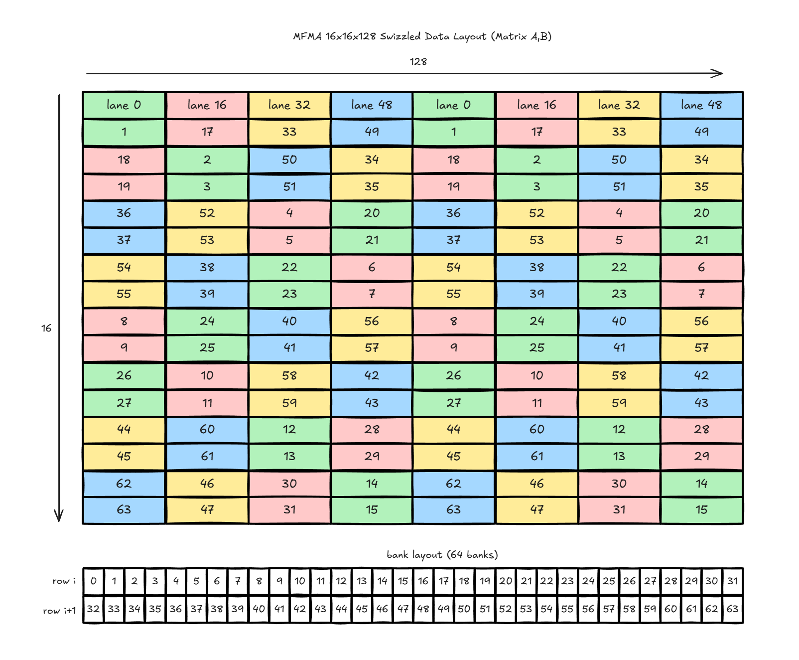
Figure 5: Swizzled LDS Access#
After swizzling, lanes are redistributed so that threads within one phase access different banks.
The performance after swizzling:
Direct global-to-LDS load path:
0.27125 ms,506.70 TFLOPS/sDirect global-to-LDS load + swizzle path:
0.27630 ms,497.43 TFLOPS/sDelta:
+0.00505 ms/-9.27 TFLOPS/s(-1.83%)
Why is throughput almost unchanged, after resolving bank conflicts? The short answer is that this stage is no longer dominated only by LDS bank conflicts: fetch/compute serialization still leaves MFMA idle windows, and swizzle index computation also adds instruction overhead.
Software Pipelining with Double Buffering#
After resolving bank conflicts, the remaining bottleneck is serialized computation: each K tile is loaded, waited on, and only then consumed by the MFMA. That results in large MFMA idle windows, as the side-by-side timelines in Figure 6 make clear.

Figure 6: Single-Buffer Load Workflow vs. Double-Buffer Load Workflow#
Figure 6 compares both timelines in one view: single buffer (left) vs double buffer (right). In the single-buffer path, global-to-LDS movement and MFMA are mostly sequential (load -> wait/sync -> compute). In this case, one thread block runs 4 waves (2x2 wave layout), and all 4 waves share the same LDS tile region, so the next tile cannot be staged until the current compute drains across the block.
The next step uses ping-pong LDS buffering:
Keep two LDS slots for each operand: one slot is being computed, the other slot is being filled with the next K tile.
Start with a prologue load of tile 0 into slot 0, then synchronize once.
In each loop step, launch load for tile
t+1into the other slot while computing tiletfrom the current slot.At tile boundary, wait for the next load to complete, synchronize, then swap slots.
All 4 waves in the block follow the same slot switch so they stay aligned on the same tile.
Double-buffered pseudo-code:
// Double-buffered with K-tile pipeline
LdsTile A_lds[2], B_lds[2];
int cur = 0, nxt = 1;

prefetch_tile_to_lds(A_lds[cur], B_lds[cur], /*tile=*/0);
wait_for_global_loads();
block_sync();

for (int t = 0; t < num_k_tiles; ++t) {
    if (t + 1 < num_k_tiles) {
        // Overlap: load next tile while current tile is computing
        prefetch_tile_to_lds_async(A_lds[nxt], B_lds[nxt], /*tile=*/t + 1);
    }

    fragments_a = read_fragments_from_lds(A_lds[cur]);
    fragments_b = read_fragments_from_lds(B_lds[cur]);
    acc = mfma(acc, fragments_a, fragments_b);

    if (t + 1 < num_k_tiles) {
        wait_for_global_loads();
        block_sync();
        cur ^= 1;
        nxt ^= 1;
    }
}
This turns the K-tile loop into a software pipeline with a startup phase, a repeated overlap phase, and a finish phase, overlapping memory ingress of tile t+1 with MFMA compute on tile t.
In the double-buffer path, the next tile’s global-to-LDS transfer runs in parallel with current MFMA work, with only a short hand-off synchronization between tiles. Once double buffering removes more of that serialization, swizzling shows a clear gain (avg_tflops from 1056.95 without swizzle to 1166.41 with swizzle, +10.36% for M=N=K=4096). Relative to single buffer load (497.43 TFLOPS/s), the swizzled double-buffer result is 2.34x higher (+134.50%).
Occupancy and Multi-Wave Trade-offs#
At this stage, the simple idea is to give each thread block more work so the GPU stays busier. We do that in two ways:
Use more waves in one block.
Use a larger output tile per block.
Why this can help:
More waves can keep matrix-core work running with fewer idle gaps.
A larger tile can reuse loaded data more times before fetching new data.
With double buffering, a heavier compute tile gives more time to hide the next data load, so load and compute overlap better.
But there is a limit. If we push too far, each block becomes heavier (more registers, more shared-memory pressure, and more sync work), and performance can flatten or drop.
In this blog post, we compare three configurations:
Configuration |
Output tile |
Threads per block |
Waves per block |
|
M=N=K |
|---|---|---|---|---|---|
|
|
|
|
|
|
|
|
|
|
|
|
|
|
|
|
|
|
Table 4. Performance comparison of three multi-wave FP8 GEMM kernel configurations for `M=N=K=4096`.
Among the three configurations in Table 4, 256x256_t512 is the highest-performing kernel tested in this post. It achieves the highest measured TFLOPS/s while keeping block size and wave count at a balanced level. To make the algorithm design of the 256x256_t512 kernel easier to understand, the wave distribution for global-memory and LDS movement is shown in Figure 7.

Figure 7: Wave Layout in the 256x256_t512 kernel#
Figure 7 presents the full wave mapping in four views. In the top-left panel (global to LDS), all 8 waves cooperatively fill a 256x128 LDS tile for A/B as repeated narrow row strips. In the top-right panel (output tile), work is split into 64x32 wave blocks: Wave0-3 and Wave4-7 alternate by 64-row bands across the 256x128 C/D region shown. In the bottom-left panel (A: LDS to registers), reads are grouped by row bands. In the bottom-right panel (B: LDS to registers), reads are grouped by 32-row bands in fixed wave pairs: (Wave0, Wave4), (Wave1, Wave5), (Wave2, Wave6), and (Wave3, Wave7), then the same pattern repeats for the next half.
8-Wave Ping-Pong Scheduling#
In the last optimization step we will modify instruction scheduling in our 256x256_t512 kernel following the 8-wave ping-pong pattern introduced in HipKittens: Fast and Furious AMD Kernels. The 8-wave ping-pong pattern employs eight waves per thread block with two waves resident per SIMD. Figure 8 shows how the two waves within each SIMD alternate between memory and MMA instructions:

Figure 8: 8-Wave Ping-Pong Scheduling Pattern#
LLVM intrinsic functions allow us to control instruction and wave scheduling.
__builtin_amdgcn_s_barrier()can be used to stall waves and increase code execution distance between them. Let’s take a look at a concrete example:
// 8 waves per threadblock (threadIdx.x = 0...511)

int waveid = threadIdx.x / 64; // waveid = 0...7
int wave_m = waveid / 4; // wave_m = 0...1
int wave_n = waveid % 4; // wave_n = 0...3

// code block 0
// ...

if (wave_m == 1) {
    __builtin_amdgcn_s_barrier(); // barrier 0
}

// code block 1
// ...

__builtin_amdgcn_s_barrier(); // barrier 1

// code block 2
// ...
In this example, eight waves per thread block are used. Waves 0 and 4 are scheduled on SIMD 0, waves 1 and 5 on SIMD 1, waves 2 and 6 on SIMD 2, and waves 3 and 7 on SIMD 3. Initially, all eight waves execute code block 0 simultaneously. After reaching barrier 0, waves 4, 5, 6, and 7 stall, while waves 0, 1, 2, and 3 continue executing code block 1. When waves 0, 1, 2, and 3 reach barrier 1, they release waves 4, 5, 6, and 7, which then proceed to execute code block 1. Meanwhile, waves 0, 1, 2, and 3 move on to execute code block 2, and so on. In this way, we can achieve alternate behaviour between two waves within one SIMD.
__builtin_amdgcn_s_setprio(x)controls how waves are scheduled and executed on the CUs at compile-time. When competing for hardware resources, the CU will, at runtime, choose the wavefront with the higher priority. Possiblexvalues are 0-3.__builtin_amdgcn_sched_barrier(x)controls the types of instructions that may be allowed to cross the intrinsic during instruction scheduling. The parameter is a mask for the instruction types that can cross the intrinsic.__builtin_amdgcn_sched_barrier(0)means no instructions may be scheduled acrosssched_barrier.
With these LLVM intrinsic functions we can implement the 8-wave ping- pong kernel. The algorithm design follows the FP8 GEMM kernel presented in HipKittens: Fast and Furious AMD Kernels. Pseudo-code of the kernel is shown below. As can be seen from the code, after the prologue, one wave within SIMD issues buffer load and LDS memory instructions, while the second wave within the SIMD executes MFMA instructions. Then they swap roles, flipping back and forth between compute and memory instructions. We use #pragma unroll 2 for the main loop, to reduce register pressure and eliminate register spilling. After the hot loop completes, some memory instructions are still in flight. Therefore, the final two k iterations must be manually unrolled. This is handled in the epilogue, which is omitted from the code here for readability.
__shared__ fp8 A_lds [2][2][128*128] // A_lds [x][0][x] - first 128x128 block, A_lds [x][1][x] - second 128x128 block
__shared__ fp8 B_lds [2][2][128*128]

fp8 a_reg[4][32]
fp8 b_reg0[2][32]
fp8 b_reg1[2][32]

float c_reg0[8][4] = 0
float c_reg1[8][4] = 0
float c_reg2[8][4] = 0
float c_reg3[8][4] = 0

int waveid = threadIdx.x / 64; // waveid = 0...7
int wave_m = waveid / 4; // wave_m = 0...1
int wave_n = waveid % 4; // wave_n = 0...3

int tic = 0;
int toc = 1;

// PROLOGUE
// Initial values: vmcnt = 0, lgkmcnt = 0

issue async buffer loads: vmem -> B_lds[tic][0] // vmcnt += 2
issue async buffer loads: vmem -> A_lds[tic][0] // vmcnt += 2
issue async buffer loads: vmem -> B_lds[tic][1] // vmcnt += 2
issue async buffer loads: vmem -> A_lds[tic][1] // vmcnt += 2

if (warp_m == 1) {
    __builtin_amdgcn_s_barrier(); // waveid=4,5,6,7 stall
}

asm volatile("s_waitcnt vmcnt(4)"); // wait until there are only 4 vmem loads remain in flight
__builtin_amdgcn_s_barrier();

issue async buffer loads: vmem -> A_lds[toc][0] // vmcnt += 2
issue async buffer loads: vmem -> B_lds[toc][0] // vmcnt += 2
issue async buffer loads: vmem -> B_lds[toc][1] // vmcnt += 2

asm volatile("s_waitcnt vmcnt(6)"); // wait until there are only 6 vmem loads remain in flight
__builtin_amdgcn_s_barrier();
// END PROLOGUE

// HOT LOOP
#pragma unroll 2
for (int k=0; k<K/128 - 2; k+=1; tic^=1, toc^=1) {
    issue async ds_read_b128 reads: B_lds[tic][0] -> b_reg0 // lgkmcnt += 4
    issue async ds_read_b128 reads: A_lds[tic][0] -> a_reg // lgkmcnt += 8
    issue async buffer loads: vmem -> A_lds[toc][1] // vmcnt += 2
    asm volatile("s_waitcnt lgkmcnt(8)"); // wait until there are only 8 lds loads remain in flight
    __builtin_amdgcn_s_barrier();

    asm volatile("s_waitcnt lgkmcnt(0)"); // wait until all lds loads are finished
     __builtin_amdgcn_s_setprio(1);
    c_reg0 += mma(a_reg, b_reg0); // Matrix Core instructions
    __builtin_amdgcn_s_setprio(0);
    __builtin_amdgcn_s_barrier();
    __builtin_amdgcn_sched_barrier(0);

    issue async ds_read_b128 reads: B_lds[tic][1] -> b_reg1 // lgkmcnt += 4
    issue async buffer loads: vmem -> A_lds[tic][0] // vmcnt += 2
    __builtin_amdgcn_s_barrier();

    asm volatile("s_waitcnt lgkmcnt(0)"); // wait until all lds loads are finished
     __builtin_amdgcn_s_setprio(1);
    c_reg1 += mma(a_reg, b_reg1); // Matrix Core instructions
    __builtin_amdgcn_s_setprio(0);
    __builtin_amdgcn_s_barrier();

    issue async ds_read_b128 reads: A_lds[tic][1] -> a_reg // lgkmcnt += 8
    issue async buffer loads: vmem -> B_lds[tic][0] // vmcnt += 2
    __builtin_amdgcn_s_barrier();

    asm volatile("s_waitcnt lgkmcnt(0)"); // wait until all lds loads are finished
     __builtin_amdgcn_s_setprio(1);
    c_reg2 += mma(a_reg, b_reg0); // Matrix Core instructions
    __builtin_amdgcn_s_setprio(0);
    __builtin_amdgcn_s_barrier();
    __builtin_amdgcn_sched_barrier(0);

    issue async buffer loads: vmem -> B_lds[tic][1] // vmcnt += 2
    asm volatile("s_waitcnt vmcnt(6)");
    __builtin_amdgcn_s_barrier();

    __builtin_amdgcn_s_setprio(1);
    c_reg3 += mma(a_reg, b_reg1); // Matrix Core instructions
    __builtin_amdgcn_s_setprio(0);
    __builtin_amdgcn_s_barrier();
}
// END HOT LOOP

// EPILOGUE (last two K iterations) skipped for readability
// ...
/// END EPILOGUE

write c_reg0, c_reg1, c_reg2, c_reg3 to vmem
Results#
All measurements in this section were collected on the same test setup and methodology described in the note below [1]. Table 5 summarizes how each optimization step changes runtime and throughput.
Kernel |
Configuration |
Avg ms |
|
M=N=K |
|---|---|---|---|---|
Baseline |
Naive global-memory mapping |
|
|
|
LDS tiling |
Shared-memory tile reuse |
|
|
|
Matrix-core baseline |
Matrix-core compute path |
|
|
|
Vectorized ingress |
Matrix-core + vectorized load |
|
|
|
Direct global-to-LDS ingress |
Matrix-core + direct global-to-LDS load |
|
|
|
LDS swizzle |
Direct global-to-LDS load + swizzle |
|
|
|
Double buffering |
Overlapped load/compute pipeline |
|
|
|
Multi-wave option A |
|
|
|
|
Multi-wave option B |
|
|
|
|
Multi-wave option C |
|
|
|
|
8-Wave Ping-Pong Scheduling |
|
|
|
|
hipBLASLt |
|
|
|
|
8-Wave Ping-Pong Scheduling |
|
|
|
|
hipBLASLt |
|
|
|
Table 5. End-to-end runtime and throughput across FP8 GEMM kernel optimization stages and the hipBLASLt baseline.
Figure 9 pulls the optimization path together: each step improves throughput, and the final kernel approaches hipBLASLt.
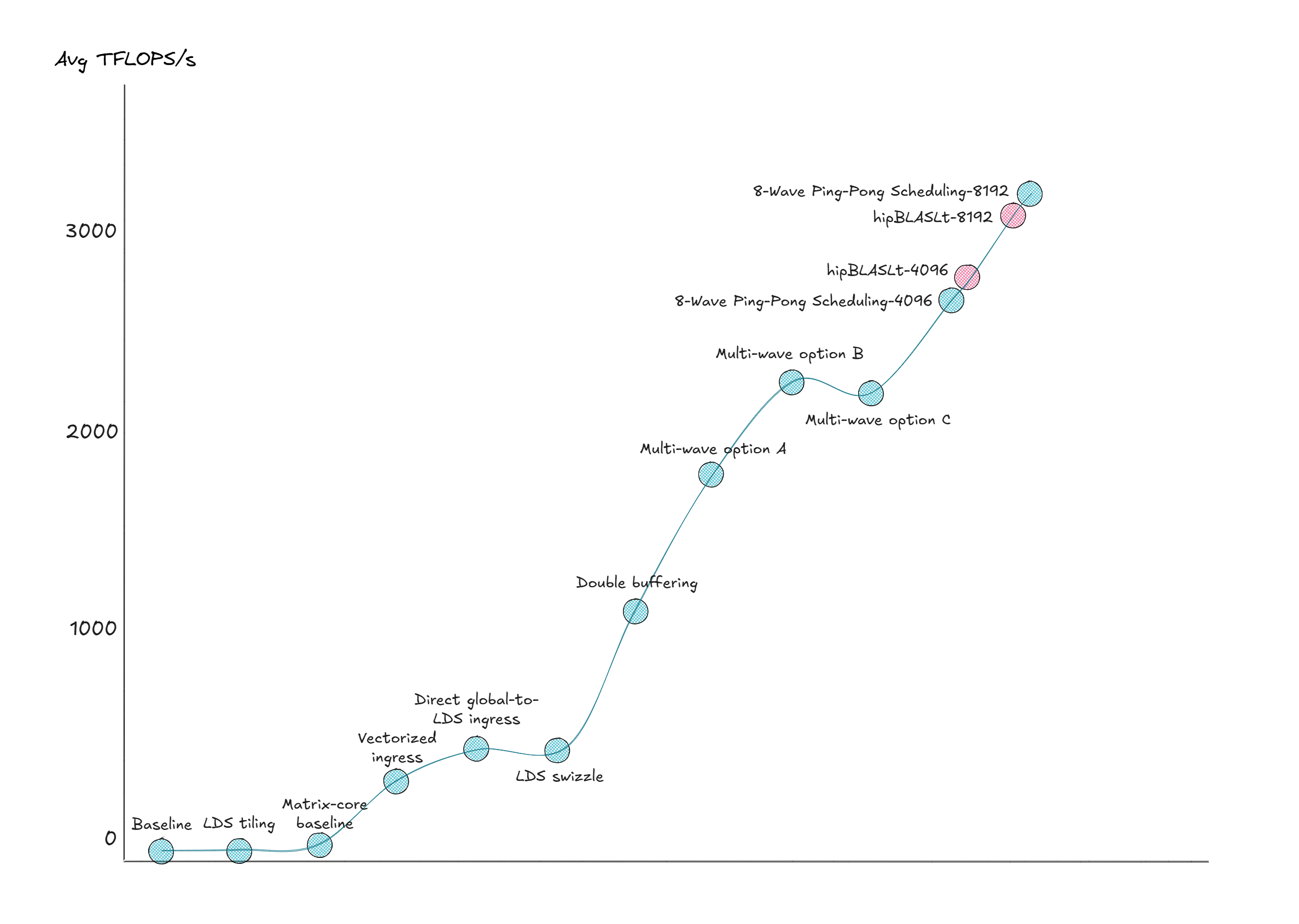
Figure 9: Results Performance Comparison#
Summary#
In this blog post, we walk through the step-by-step optimization of an FP8 GEMM kernel on the AMD Instinct MI355X GPU. By applying techniques such as double buffering, Matrix Core instructions, LDS swizzled memory access, fine-grained instruction scheduling, and the 8-wave ping-pong algorithm design, we were able to achieve performance comparable to hipBLASLt. Importantly, this was accomplished without writing the kernel in assembly; instead, we remained at the HIP/C++ level throughout the process. During the optimization work, we also gained hands-on experience using compiler intrinsic functions and inline assembly within HIP kernels to achieve better control over instruction selection and scheduling.
Notes#
SYSTEM CONFIGURATION: AMD Instinct™ MI355X platform#
GPU: AMD Instinct™ MI355X (
gfx950)ROCm stack: ROCm 7.1.0
Workload: FP8 GEMM (
E4M3FN) with BF16 output and FP32 accumulation, matrix sizesM=N=K=4096and8192Methodology: warm-up iterations and measured iterations as shown earlier; TFLOPS/s computed using
2MNK/t
Disclaimers#
Third-party content is licensed to you directly by the third party that owns the content and is not licensed to you by AMD. ALL LINKED THIRD-PARTY CONTENT IS PROVIDED “AS IS” WITHOUT A WARRANTY OF ANY KIND. USE OF SUCH THIRD-PARTY CONTENT IS DONE AT YOUR SOLE DISCRETION AND UNDER NO CIRCUMSTANCES WILL AMD BE LIABLE TO YOU FOR ANY THIRD-PARTY CONTENT. YOU ASSUME ALL RISK AND ARE SOLELY RESPONSIBLE FOR ANY DAMAGES THAT MAY ARISE FROM YOUR USE OF THIRD-PARTY CONTENT.