AMD Instinct MI455X vs MI355X: A Technical Look at the Advancing AI 2026 Inference Numbers#

At Advancing AI 2026, AMD shared a set of performance results comparing the new AMD Instinct™ MI455X (Helios) accelerator against the current-generation AMD Instinct™ MI355X. This post explains what went into those numbers: the workloads, the kernels, the test configuration, the metric definitions, and the caveats that sit behind each figure.
The results fall into two groups. The first is an end-to-end online serving benchmark on DeepSeek-V4-Flash, which is the number most representative of a real deployment. The second is a set of component microbenchmarks that isolate compute, memory bandwidth, and networking. The microbenchmarks explain where the serving gains come from, and each one measures a single behavior under controlled conditions.
Throughout this post we present results as MI455X-to-MI355X ratios, and where charts are shown we normalize throughput to the MI355X peak. Every ratio maps back to median measurements in the underlying test data.
Prerequisites#
This post assumes some familiarity with LLM inference. You will get the most out of it if you are comfortable with:
The two phases of inference: prefill (processing the input prompt in parallel) and decode (generating output tokens sequentially, one at a time).
Online serving metrics, including concurrency, total throughput, and per-user token rate.
GPU performance fundamentals: what a GEMM is, the distinction between compute-bound and memory-bandwidth-bound kernels, and why HBM bandwidth matters for the decode phase.
Basic multi-GPU concepts: scale-up (communication within the tightly-coupled GPU domain) versus scale-out (communication beyond that domain, across the external fabric).
We define the model-specific and benchmark-specific terms as they come up, and we link to the public documentation for every tool and library named. You do not need access to AMD Instinct hardware to follow the methodology.
How to Read These Numbers#
A few conventions apply across all of the results.
Medians, not single runs. Each microbenchmark was executed five times, and we report the median of the five runs. This reduces the effect of run-to-run variation from thermal state, clock residency, and system noise.
Single-GPU comparisons. Every result compares one MI455X GPU against one MI355X GPU. The MI355X system used for testing contains eight GPUs, and these tests exercised a single GPU so the comparison stays at the per-accelerator level. The two exceptions are the networking benchmarks, which by definition involve more than one endpoint.
MI455X ran on a pre-release Helios bringup platform. Software enablement for MI455X is still maturing. The numbers reflect a specific point in bringup, and later ROCm and framework releases may move them.
These are point-in-time results. Both MI455X and MI355X continue to improve as their software stacks mature, so treat every ratio here as a snapshot rather than a fixed relationship. Your own results will depend on your software versions, workloads, and system configuration.
Two comparison styles. Some benchmarks use an identical configuration on both GPUs, which we call apples-to-apples. Others use a configuration individually tuned for each GPU, which we call peak-to-peak. The distinction matters for interpretation, so we call it out for each benchmark below.
End-to-End: DeepSeek-V4-Flash Online Serving#
This is the result that best represents a production inference deployment.
The Model and the Framework#
DeepSeek-V4-Flash is an open-source Mixture-of-Experts (MoE) model with 284B total parameters and 13B activated per token. In an MoE model, a router selects a small subset of expert subnetworks for each token, so only the activated parameters contribute to the compute cost of that token. Expert weights are stored in FP4 precision, and most other parameters are in FP8. The model supports context lengths up to one million tokens, and it is compact enough to serve effectively on a single GPU, which makes it a clean subject for a per-GPU generational comparison. Both the MI455X and MI355X tests served the model through AMD’s ATOM inference stack on a single GPU.
The Two Metrics#
Online serving performance is a trade-off between two quantities:
Interactivity is output tokens per second per user. It measures how responsive each individual user’s stream feels. Higher is better.
Total token throughput per GPU is the aggregate token rate the GPU sustains across all concurrent users. Higher is better.
As you increase the number of concurrent requests, total throughput rises while per-user interactivity falls. Sweeping concurrency therefore traces a throughput-versus-interactivity curve for each GPU. We ran this sweep at two fixed sequence-length settings:
1K/1K: 1,024-token input, 1,024-token output. This is a balanced prefill-to-decode ratio and a common default operating point.
1K/8K: 1,024-token input, 8,192-token output. This is a generation-heavy workload where the decode phase dominates, which shows how the comparison shifts under a much longer output.
How the Ratio Is Computed#
The headline “up to 34x higher token throughput at high interactivity”[1] is a throughput ratio measured at a fixed interactivity threshold. The method is worth stating precisely, because it is the fair way to compare two serving curves. AMD reports this comparison at three representative points: high interactivity (the most responsive experience, near 90 tokens/s/user), medium interactivity (near 70 tokens/s/user), and low interactivity (near 30 tokens/s/user), giving up to 34x, 17x, and 4x respectively.
For a given interactivity target, for example 60 output tokens per second per user, we find the highest total throughput each GPU can deliver while still meeting that target. The ratio at that threshold is the MI455X throughput divided by the MI355X throughput. Reading the ratio this way answers a concrete question: at the same quality of experience, how much more total work does each GPU do?
Because the two curves have different shapes, the ratio depends on the threshold. At relaxed interactivity targets both GPUs are near their throughput ceilings and the ratio is modest. At demanding targets the MI355X curve has already dropped off while MI455X is still serving a large concurrent batch, so the ratio grows.
1K/1K Results#
Figure 1 below shows the throughput-versus-interactivity curve for each GPU on this workload, and the table that follows lists the MI455X/MI355X ratio at each interactivity threshold.
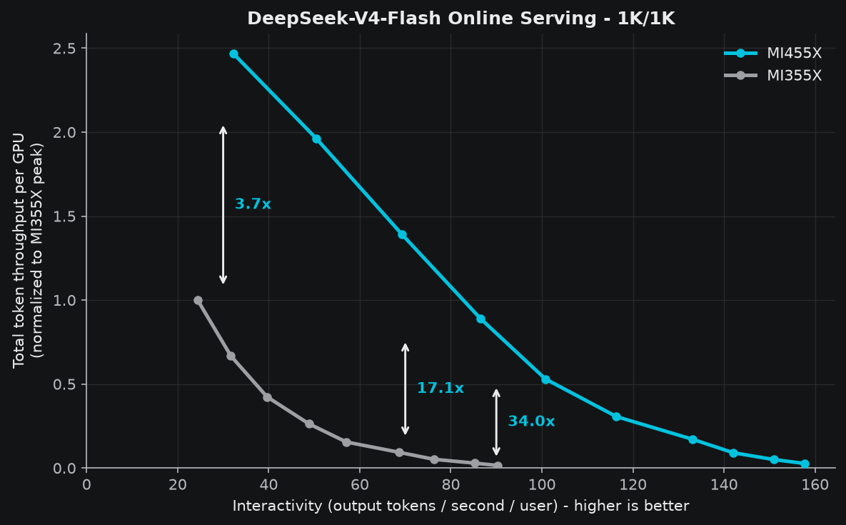
Figure 1: DeepSeek-V4-Flash online serving, 1,024-token input and 1,024-token output. Throughput per GPU is normalized to the MI355X peak. Higher and further right is better. Arrows mark the MI455X/MI355X throughput ratio at fixed interactivity thresholds.#
Interactivity threshold (tokens/s/user) |
MI455X / MI355X throughput ratio |
|---|---|
20 |
2.47x |
30 |
3.70x |
40 |
7.44x |
50 |
12.66x |
60 |
14.79x |
70 |
17.06x |
80 |
30.46x |
90 |
33.98x |
On this balanced workload the ratio climbs from under 3x at a relaxed 20 tokens/s/user target to 34x at a demanding 90 tokens/s/user target. The steepest gains come at the high-interactivity end, where the MI355X curve drops below successive concurrency steps and can no longer hold the target.
1K/8K Results#
Figure 2 repeats the sweep for the longer 8,192-token output, again with the per-threshold ratios in the table below it.
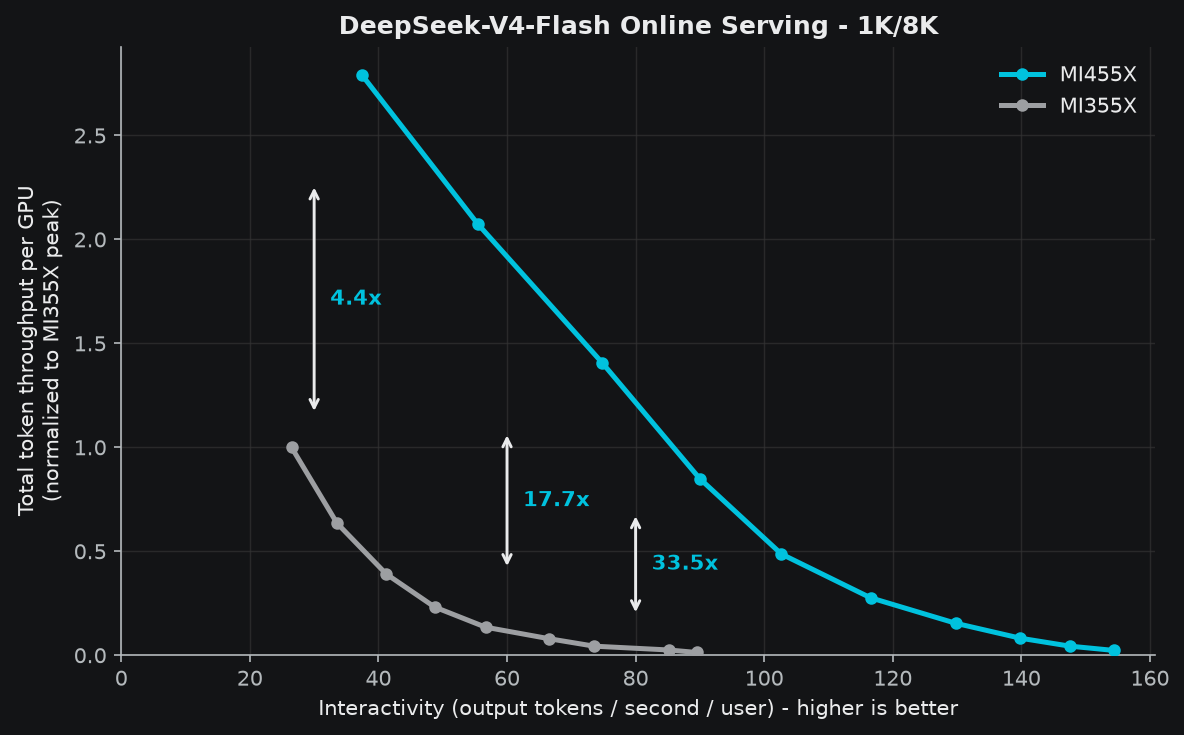
Figure 2: DeepSeek-V4-Flash online serving, 1,024-token input and 8,192-token output. Throughput per GPU is normalized to the MI355X peak. Higher and further right is better.#
Interactivity threshold (tokens/s/user) |
MI455X / MI355X throughput ratio |
|---|---|
20 |
2.79x |
30 |
4.39x |
40 |
5.30x |
50 |
15.38x |
60 |
17.74x |
70 |
32.20x |
80 |
33.52x |
Lengthening the output to 8,192 tokens makes the workload decode-heavy, and the curve follows the same shape, reaching up to 33.5x at an 80 tokens/s/user target. Both curves and their full per-concurrency data are available in the accompanying data tables. The component benchmarks below explain why MI455X holds a good experience across so much more of the concurrency range.
Compute and Memory Bandwidth#
The end-to-end serving gains rest on generational improvements in three building blocks: low-precision compute, attention-phase memory bandwidth, and raw HBM read throughput. Each is isolated below with a focused microbenchmark, then summarized together.
Compute: MXFP4 GEMM#
Matrix multiplication is the workhorse of transformer inference; it runs the attention projections, the MLP layers, and the output projections, so a low-precision GEMM kernel tells you a lot about compute-bound performance. To compare the two generations, we timed an MXFP4 GEMM from AITER, AMD’s AI operator library for ROCm, at M=4096, N=4096, K=262144, with MXFP4 inputs, BF16 compute and output, and a trigonometric (“trig”) initialization pattern. AITER hands back a TFLOPS number, which we convert to PFLOPS and report as the median of five runs.
In these tests the generational gap is wide: a single MI455X GPU reached up to 3.3x higher MXFP4 performance than a single MI355X GPU[2], a reported 20.0 PFLOPS against 6.0 PFLOPS. Results are based on specific test configurations and may vary.
Before reading too much into that number, a few things are worth knowing:
This is an apples-to-apples comparison. The same matrix shape runs on both GPUs. The shape was selected for peak MI455X performance, and other shapes may produce a somewhat higher relative figure for MI355X.
MXFP4 GEMM performance is sensitive to matrix and scale-factor initialization. The trig pattern used here was implemented with a very slow period, which made the inputs near-constant and yields a peak-delivered figure. This behavior is specific to this implementation. Trig initialization as it is usually defined in GEMM benchmarks varies faster and behaves more like a uniform random distribution, which produces lower throughput. Real-world data typically falls somewhere in between, so read this result as peak-delivered rather than typical.
Although the near-constant initialization makes this a peak-delivered result, we report a conservative 20.0 PFLOPS rather than the higher figure the microbenchmark reached. This is because real MXFP4 workloads, whose data is not near-constant, will typically land below this.
Memory Bandwidth: MLA Decode Attention#
DeepSeek-style models lean on Multi-Latent Attention (MLA), and in the decode phase that attention is bottlenecked by how fast the GPU can stream key and value state out of memory. That makes it a good place to look for a memory-bandwidth advantage. We took a bandwidth-bound MLA decode kernel from AITER, tuned it to push sustained HBM bandwidth on each GPU, and derived a TB/s figure from the number of bytes the kernel must read, divided by elapsed time, using identical byte-accounting on both parts and reporting the median of five runs.
In these tests MI455X came out ahead by up to 3.8x higher bandwidth than MI355X on this MLA benchmark[3]. The same kernel also reports a compute figure, where MI455X leads by 1.9x; the bandwidth ratio being the larger of the two is the tell that the kernel is genuinely bandwidth-bound, which is the regime decode lives in. Results are based on specific test configurations and may vary.
A note on methodology:
This is a peak-to-peak comparison. The MI455X and MI355X kernels do not use identical source code and are each tuned for their target GPU.
The kernel still performs some computation, so achieved bandwidth is below the theoretical HBM peak for either GPU.
Memory Bandwidth: HBM Read Throughput#
Underneath every bandwidth-bound phase of inference and training sits one question: how fast can the GPU read from HBM? To answer it in isolation from compute, we used an internal synthetic memory benchmark based on BabelStream, built from the same source on both GPUs with only the target architecture changed. The kernel reads a device-memory buffer sized well beyond cache, so what you are measuring is HBM and not on-chip memory, and it repeats hundreds of times back to back with a single sync at the end. Sum the bytes read, divide by the elapsed time, and you get the average throughput, again the median of five runs.
In these tests, on a pure read, MI455X achieved up to 3x higher measured HBM read throughput than MI355X[4], a direct reflection of the move from HBM3E to HBM4. Results are based on specific test configurations and may vary.
Please keep in mind these two caveats:
Maximum bandwidth requires sufficiently large transfers. Small transfers are latency-bound and will not show the same improvement.
The loop and element counts were increased relative to prior generations to sustain the higher MI455X bandwidth. A synthetic read test isolates HBM read behavior, and real workloads mix reads, writes, compute, and idle phases, which lowers achieved bandwidth.
This also explains why the MLA decode benchmark showed a larger 3.8x gain than the 3x raw HBM read improvement. On MI355X, MLA decode was partly compute-limited and could not reach full HBM bandwidth, while on MI455X it runs close to the bandwidth ceiling. That difference widens the effective memory-bandwidth gap in decode beyond the raw read-throughput ratio.
Taken together, these are broad gains across compute and memory bandwidth, and the memory-bandwidth improvements in particular are the through-line for decode-bound serving. Figure 3 collects the three microbenchmark ratios side by side, with the underlying numbers in the table that follows.
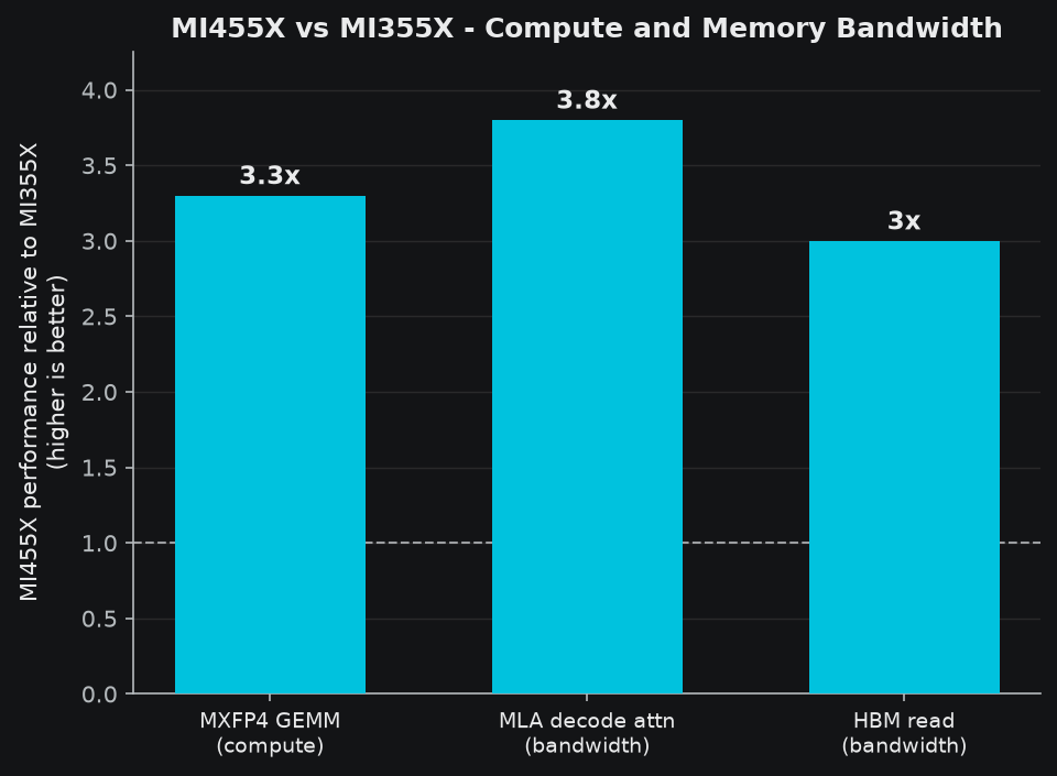
Figure 3: MI455X performance relative to MI355X on the compute and memory-bandwidth microbenchmarks. Higher is better; the dashed line is the MI355X baseline.#
Benchmark |
Category |
Tool |
MI455X / MI355X |
Comparison style |
|---|---|---|---|---|
MXFP4 GEMM |
Compute |
AITER |
up to 3.3x |
Apples-to-apples |
MLA decode attention |
Memory bandwidth |
AITER |
up to 3.8x |
Peak-to-peak |
HBM read throughput |
Memory bandwidth |
BabelStream-based |
up to 3x |
Apples-to-apples |
Networking#
Multi-GPU and multi-node workloads are gated by the fabric between GPUs, so we measure bandwidth at two levels: scale-up (GPU-to-GPU inside the tightly-coupled domain) and scale-out (across the external fabric that connects those domains). The boundary between the two is platform-specific, which we return to below. These gains matter as soon as a workload spans more than one GPU, including distributed training, MoE expert parallelism, and multi-node inference pipelines.
Scale-Up#
Scale-up is the GPU-to-GPU bandwidth inside the tightly-coupled scale-up domain, and it is what tensor-parallel and expert-parallel communication ride on as GPUs swap activations and expert outputs. We measured it with TransferBench at a 16 GB transfer size, big enough to reach steady state, comparing a 4x MI455X node against an 8x MI355X node. TransferBench separates two quantities worth keeping distinct: the total scale-up bandwidth per GPU, meaning the aggregate a single source GPU can push to all its peers at once, and the single GPU-to-GPU bandwidth, meaning one transfer between one pair. It reports each in unidirectional and bidirectional forms. Against the 8x MI355X platform, the 4x MI455X platform came in at[5]:
Metric |
MI455X / MI355X ratio |
|---|---|
Total unidirectional bandwidth per GPU |
up to 3.8x |
Single GPU-to-GPU unidirectional bandwidth |
up to 27x |
Total bidirectional bandwidth per GPU |
up to 3.7x |
Single GPU-to-GPU bidirectional bandwidth |
up to 26x |
Those two numbers tell different stories. The roughly 3.8x on aggregate per-GPU bandwidth is the plain generational gain in total fabric bandwidth. The single GPU-to-GPU figure is far larger because of a topology change: MI455X uses a switched scale-up fabric, so one GPU can aim its entire bandwidth at a single peer, whereas on MI355X the per-GPU total is spread across several parallel links and any one pairwise transfer sees only a slice of it. So treat the single-pair figure as a statement about transfers under a switched topology, and reach for the 3.8x when you are reasoning about aggregate, all-to-all communication.
One thing to keep in mind: bandwidth here scales with transfer size, and the numbers can move with fabric configuration and system state.
Scale-Out#
Push past the scale-up domain and the external fabric becomes the limiter, which is what governs distributed training and multi-node inference. To measure this node-to-node bandwidth we ran ib_write_bw from the RDMA perftest package in bidirectional mode, so both endpoints issue RDMA writes at once and the figure reported is the combined two-way throughput. The MI455X node carried an AMD Pensando™ Vulcano 800 NIC and the MI355X node an AMD Pensando™ Pollara 400 NIC, and we took the median bidirectional bandwidth in Gb/s over at least 28 measurements per platform, one NIC on each side.
In these tests, with the Vulcano 800, MI455X achieved up to 2x higher bidirectional scale-out bandwidth than MI355X with the Pollara 400[6]. Results are based on specific test configurations and may vary.
Like any focused micro-benchmark, ib_write_bw reports available fabric bandwidth rather than end-to-end application performance, and the result depends on NIC firmware, driver, PCIe placement, MTU, congestion control, and switch configuration.
The size of the scale-up domain differs by platform, which changes how these two numbers apply. On MI355X, scale-up spans the 8 GPUs within a node and scale-out handles communication between nodes. On the MI455X Helios platform the scale-up domain covers an entire 72-GPU rack, and a transfer between two GPUs runs through the switch at the same bandwidth whether or not they sit in the same node, so scale-out only comes into play between racks. This shifts the practical picture. While MI455X shows up to 2x higher scale-out bandwidth, most deployments, and inference in particular, keep their communication inside the rack, where it runs at the much higher scale-up bandwidth of up to 3.8x aggregate and up to 27x single-pair.
Across both levels, the networking gains are substantial, with the largest coming from the switched scale-up topology and the rest from the generational increase in fabric bandwidth. Figure 4 brings the scale-up and scale-out ratios together, and the table beneath it breaks them out by metric.
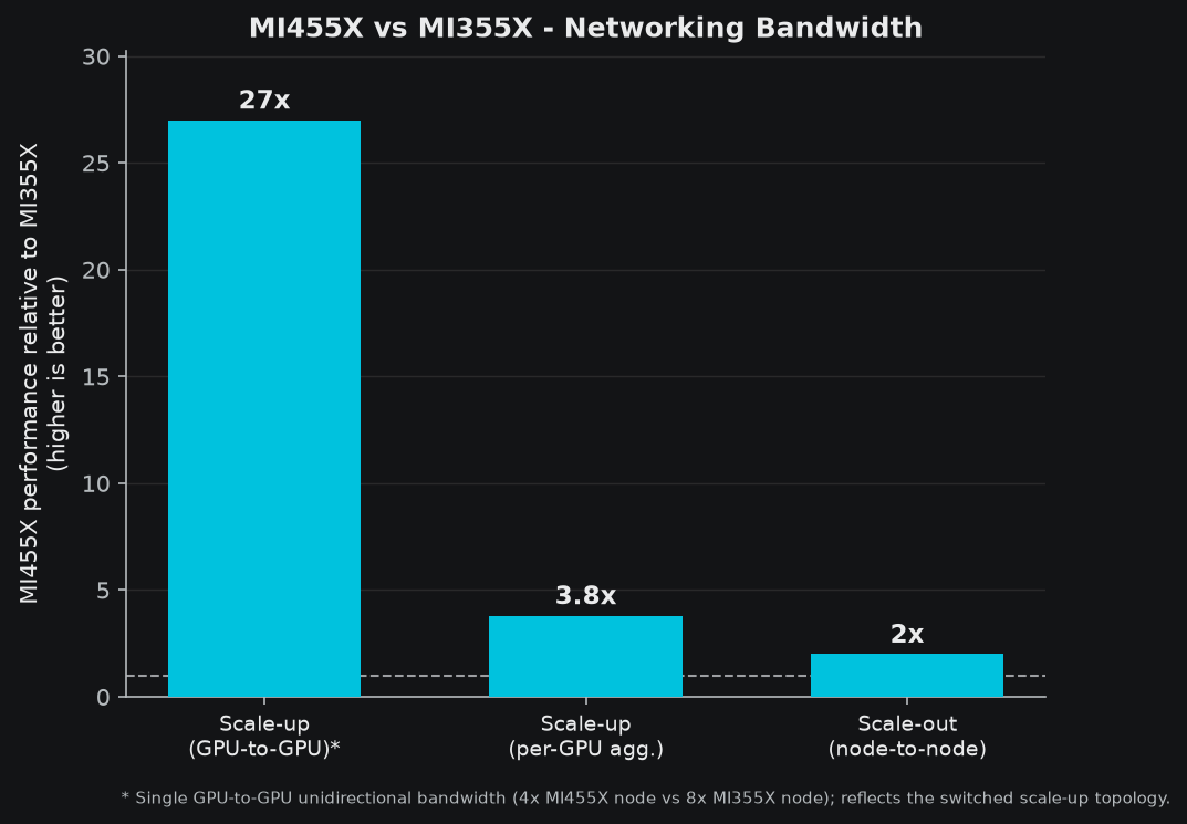
Figure 4: MI455X performance relative to MI355X on the networking microbenchmarks. Higher is better; the dashed line is the MI355X baseline. The scale-up single GPU-to-GPU figure reflects the switched topology; aggregate per-GPU scale-up uplift is about 3.8x.#
Benchmark |
Metric |
Tool |
MI455X / MI355X |
Comparison style |
|---|---|---|---|---|
Scale-up |
Single GPU-to-GPU |
TransferBench |
up to 27x |
Topology-dependent |
Scale-up |
Aggregate per GPU |
TransferBench |
up to 3.8x |
Apples-to-apples |
Scale-out |
Node-to-node |
ib_write_bw |
up to 2x |
Apples-to-apples |
Putting It Together#
Taking a step back and viewing all of the benchmarks, they tell one cohesive story. DeepSeek-V4-Flash decode is bound by memory bandwidth, and the 3.0x to 3.8x memory-bandwidth advantage is what lets MI455X sustain higher per-user token rates as concurrency climbs. Its 3.3x FP4 compute advantage keeps prefill and projection work from becoming the bottleneck, and once the model is sharded across GPUs or nodes, the scale-up and scale-out gains keep communication off the critical path. That is why the end-to-end serving multipliers exceed any single component ratio: these advantages compound across the phases of a real serving workload, and the comparison is drawn at a fixed quality of experience where the MI355X curve has already saturated. Real serving performance is the product of many gains working together, and the best way to understand it is to measure each one and then watch how they combine. If there’s one thing to take away from this blog it’s this: in the generational leap from MI355X to MI455X, every component contributing to performance under the hood has been taken to the next level, and holistic real world performance is greater than the sum of its parts.
Summary#
In this blog you followed one generational comparison from the top down, beginning with the result that matters most in production and then opening up the hardware that produces it. You saw a single MI455X GPU deliver up to 34x higher token throughput than a single MI355X GPU at high interactivity on DeepSeek-V4-Flash online serving, with about 17x at medium and 4x at low interactivity[1], and you saw why that headline depends on the interactivity target you choose to hold fixed. From there you decomposed the gain into its building blocks: up to 3.3x on MXFP4 GEMM compute[2], up to 3.8x on MLA decode bandwidth[3], and up to 3x on raw HBM read throughput[4] as HBM3E gives way to HBM4, followed by up to 3.8x aggregate and up to 27x single-pair scale-up bandwidth across a switched fabric[5] and up to 2x scale-out bandwidth between nodes[6]. Just as important, you saw how each of those numbers was defined, measured as the median of repeated runs, and normalized, so none of the claims here rests on a single unqualified figure.
If you arrived wanting to know whether a headline number holds up under scrutiny, you now have what you need to judge it for yourself: the metric definitions, the two comparison styles, and the reasoning that connects a component ratio to an end-to-end result. Every number here is a point-in-time snapshot; both accelerators keep gaining as their software stacks mature, so keep in mind that these ratios will continue to move. Follow the ROCm Blogs to stay up to date on how these results evolve.
Additional Resources#
Disclaimers#
Results are based on specific test configurations and may vary. These benchmarks were conducted by the AMD Datacenter GPU Performance Team under specific test conditions on pre-release hardware and software. Performance may vary with system configuration, software and firmware versions, workload characteristics, operating temperature, and system load. Some test images and internal tooling used to generate these results are not available externally.
The information presented in this document is for informational purposes only and may contain technical inaccuracies, omissions, and typographical errors. The information contained herein is subject to change and may be rendered inaccurate for many reasons, including but not limited to product and roadmap changes, component and motherboard version changes, new model and/or product releases, product differences between differing manufacturers, software changes, BIOS flashes, firmware upgrades, or the like. Any computer system has risks of security vulnerabilities that cannot be completely prevented or mitigated. AMD assumes no obligation to update or otherwise correct or revise this information. However, AMD reserves the right to revise this information and to make changes from time to time to the content hereof without obligation of AMD to notify any person of such revisions or changes.
THIS INFORMATION IS PROVIDED “AS IS.” AMD MAKES NO REPRESENTATIONS OR WARRANTIES WITH RESPECT TO THE CONTENTS HEREOF AND ASSUMES NO RESPONSIBILITY FOR ANY INACCURACIES, ERRORS, OR OMISSIONS THAT MAY APPEAR IN THIS INFORMATION. AMD SPECIFICALLY DISCLAIMS ANY IMPLIED WARRANTIES OF NON-INFRINGEMENT, MERCHANTABILITY, OR FITNESS FOR ANY PARTICULAR PURPOSE. IN NO EVENT WILL AMD BE LIABLE TO ANY PERSON FOR ANY RELIANCE, DIRECT, INDIRECT, SPECIAL, OR OTHER CONSEQUENTIAL DAMAGES ARISING FROM THE USE OF ANY INFORMATION CONTAINED HEREIN, EVEN IF AMD IS EXPRESSLY ADVISED OF THE POSSIBILITY OF SUCH DAMAGES.
Third-party content is licensed to you directly by the third party that owns the content and is not licensed to you by AMD. ALL LINKED THIRD-PARTY CONTENT IS PROVIDED “AS IS” WITHOUT A WARRANTY OF ANY KIND. USE OF SUCH THIRD-PARTY CONTENT IS DONE AT YOUR SOLE DISCRETION AND UNDER NO CIRCUMSTANCES WILL AMD BE LIABLE TO YOU FOR ANY THIRD-PARTY CONTENT. YOU ASSUME ALL RISK AND ARE SOLELY RESPONSIBLE FOR ANY DAMAGES THAT MAY ARISE FROM YOUR USE OF THIRD-PARTY CONTENT.
AMD, the AMD Arrow logo, AMD Instinct, AMD CDNA, AMD Pensando, and combinations thereof are trademarks of Advanced Micro Devices, Inc. Other product names used in this publication are for identification purposes only and may be trademarks of their respective companies.
© 2026 Advanced Micro Devices, Inc. All rights reserved.