Deep Dive Into 4-Wave Interleave FP8 GEMM#

Our previous two posts in this GEMM optimization series covered Matrix Core instructions and 8-wave ping-pong FP8 GEMM design. Here we discuss another algorithm design introduced by HipKittens - 4-wave interleave, which further improves the performance of the 8-wave ping-pong implementation. For the most complete understanding, we recommend reading this post alongside the source code.
One Wave Per SIMD#
To understand why 4-Wave Interleave exists, recall how the 8-Wave kernel worked: it placed two waves on each SIMD unit — one handling MFMA, one handling memory loads. These two waves alternate between memory and MMA instructions (“ping-pong”), and the hardware scheduler overlaps them because they use different hardware units.
4-Wave Interleave takes the opposite approach. It places one wave per SIMD, and that single wave is responsible for issuing both MFMA and memory instructions but in a very carefully hand-crafted order.
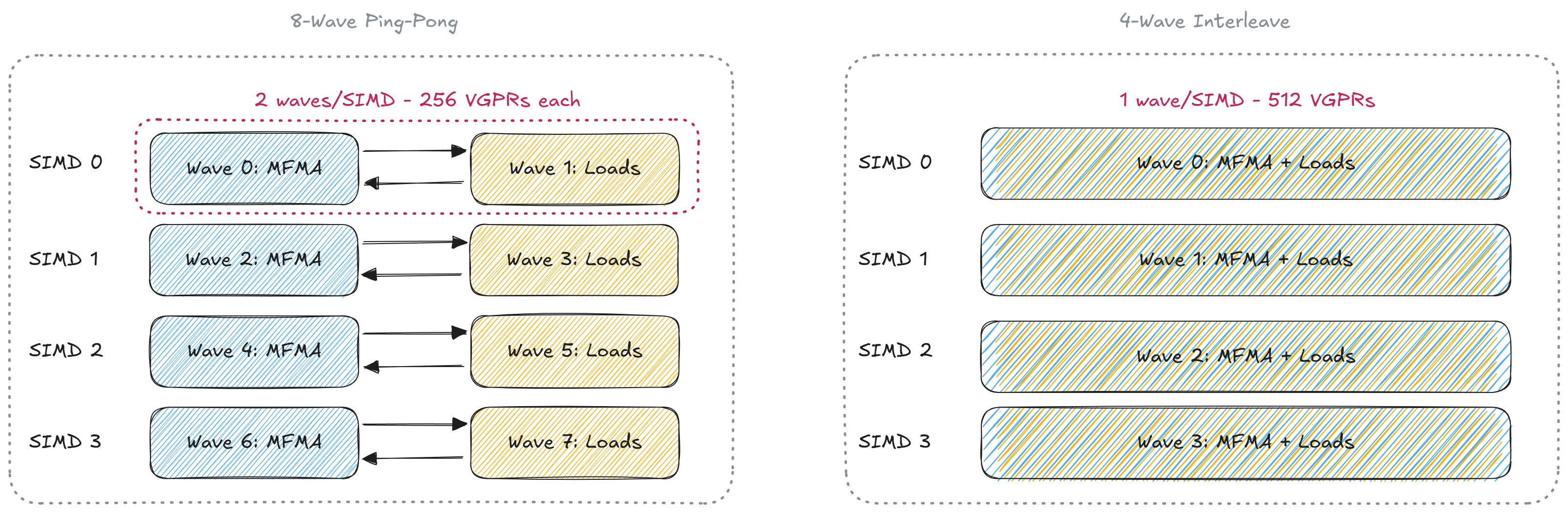
Figure 1: Wave assignment per CU#
With only one wave on the SIMD, that wave gets all 512 VGPRs compared to the 8-Wave kernel where the register budget was half that. Doubling the register file means the wave can hold a complete 128×128 output register tile at once, compared to 64×128 in the 8-wave case.
The 4-Wave and 8-Wave designs differ in their implementation complexity. The 8-Wave kernel requires creating alternating wave behavior via conditional __builtin_amdgcn_s_barrier(), whereas the 4-Wave employs a finer-grained software pipeline that overlaps memory and MFMA instructions.
Algorithm Breakdown#
In this section, we discuss the code and the implementation in detail.
For the 4-Wave kernel we will keep the same tile sizes as we used in the 8-Wave example from our previous article that is: 256x256x128. Also, we will only consider input matrices with dimensions that are multiples of the blocking parameters.
Figure 2 shows how the matrices are tiled with the parameters we just defined:
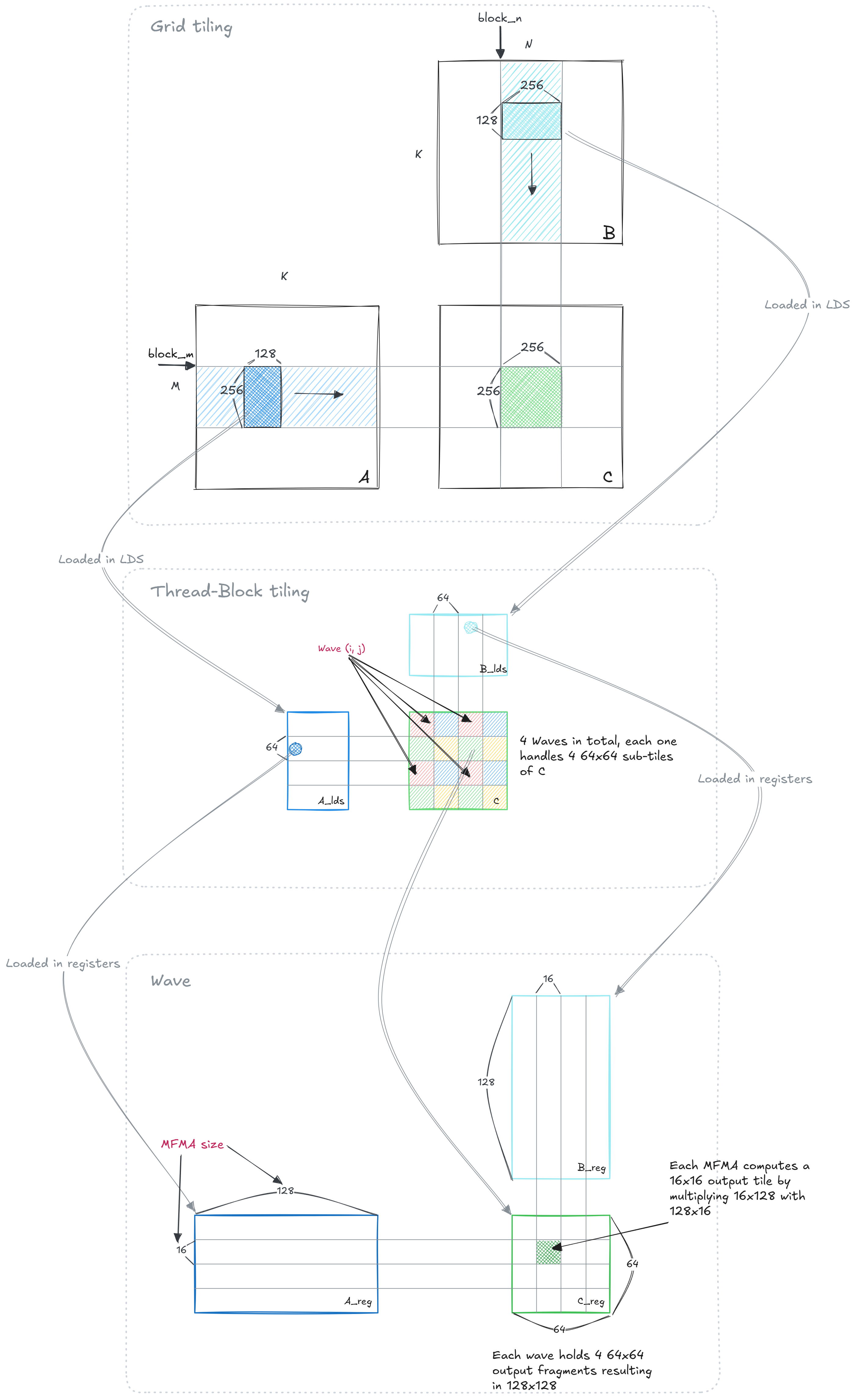
Figure 2: Algorithm structure#
Each wave ends up handling 4 64x64 tiles of the output matrix C, and each one of these is made up of a sequence of smaller, 16x16, sub-tiles. Using these smaller sub-tiles is the key that enables the interleaving: instead of issuing bulk MFMA instructions to compute, e.g., an entire 64x64 tile, we will issue smaller 16x16 MFMA instructions and mix them with memory instructions, creating custom software pipeline schemes. The idea is that by the time we finish processing an entire 64x64 tile of C, we will have already loaded the operands for the next one.
The code follows this structure:
// A/B tiles in LDS are 256x128 with double buffering, split in two 128x128
__shared__ fp8 A_lds[2][2][128 * 128];
__shared__ fp8 B_lds[2][2][128 * 128];

RT_C c[2][2]{};
RT_A a[2]{};
RT_B b[2]{};

// Compute on cur load on next
int cur = 0, next = 1;

// PROLOGUE
// Load a 256x128 tile of A and B
// load A_lds[cur] from A (global -> LDS)
// load B_lds[cur] from B (global -> LDS)

// Pre-load the next 256x128 tile of A and B
// load A_lds[next] from A (global -> LDS)
// load B_lds[next] from B (global -> LDS)

// Pre-load registers
// load a[0] from A_lds[cur][0] (LDS -> register)
// load b[0] from B_lds[cur][0] (LDS -> register)

// MAIN LOOP
for (int k = 0; k < K_BLOCKS - 2; ++k) {
    interleaved_block(
        A_lds[cur][0],  // Where to store the next 128x128 tile in LDS
        A,              // Where to load the next 128x128 tile from global memory
        b[1],           // Where to store the next 64x128 sub-tile in registers
        B_lds[cur][1],  // Where to load the next 64x128 from LDS
        a[0], b[0],     // Current MFMA operands (already in registers)
        c[0][0]         // Accumulator tile
    );

    // The remaining calls follow the same structure, rotating which buffer is being filled

    interleaved_block(B_lds[cur][0], B, a[1], A_lds[cur][1], a[0], b[1], c[0][1]);  // c[0][1] += a[0] * b[1]

    interleaved_block(B_lds[cur][1], B, a[0], A_lds[next][0], a[1], b[0], c[1][0]); // c[1][0] += a[1] * b[0]

    interleaved_block(A_lds[cur][1], A, b[0], B_lds[next][0], a[1], b[1], c[1][1]); // c[1][1] += a[1] * b[1]

    // Swap cur with next
    cur ^= 1;
    next ^= 1;
}

// EPILOGUE
// Last two iterations (k = K_BLOCKS - 2, k = K_BLOCKS - 1) + store
The core of the kernel is interleaved_block. Each call does three things:
Issues 16 MFMA instructions (a 4x4 grid of 16x16x128 MFMA) computing a 64x64 part of C.
Issues 8 LDS → register loads (loading a 64x128 fragment of A/B) to prepare the operands for the next call.
Issues 4 global → LDS loads loading a 128x128 sub-tile of A/B that will be used in the next call to bring the operands from LDS to registers.
The key mechanism is __builtin_amdgcn_sched_barrier(x), which prevents the compiler from
reordering instructions across the barrier. The parameter x is a mask that tells the compiler
which types of instructions can cross the intrinsic in the compiled schedule. x=0 means no instruction can cross the barrier.
Without it, the compiler might legally batch all memory
instructions after all MFMA, eliminating the overlap. With it, memory instructions are placed between MFMA:
// All operands (a, b, c) are already in registers when this function is called.

__builtin_amdgcn_sched_barrier(0);
mfma_ABt(c, a, b, c, 0, 0);                          // MFMA tile (row=0, col=0)
__builtin_amdgcn_sched_barrier(0);

precompute_addresses<K>(/* ... */);                  // scalar address setup

__builtin_amdgcn_sched_barrier(0);
mfma_ABt(c, a, b, c, 0, 1);                          // MFMA tile (row=0, col=1)
__builtin_amdgcn_sched_barrier(0);

precompute_swizzle_lds(lds_swizzle, wave_idx);       // scalar swizzle

load_one_lds<0>(addresses, global_offsets);          // global -> LDS
load_one_rt<0, 0>(lds_src, rt_dst, lds_swizzle);     // LDS -> rt_dst (1st 16 values)

__builtin_amdgcn_sched_barrier(0);
mfma_ABt(c, a, b, c, 0, 2);                          // MFMA tile (row=0, col=2)
__builtin_amdgcn_sched_barrier(0);

load_one_rt<0, 1>(lds_src, rt_dst, lds_swizzle);     // LDS -> rt_dst (last 16 values)

__builtin_amdgcn_sched_barrier(0);
mfma_ABt(c, a, b, c, 0, 3);                          // MFMA tile (row=0, col=3)
__builtin_amdgcn_sched_barrier(0);

load_one_lds<1>(addresses, global_offsets);
load_one_rt<1, 0>(lds_src, rt_dst, lds_swizzle);

// ... pattern continues for rows 1, 2, 3
Prologue and Epilogue#
The prologue loads both cur and next tile pairs into LDS before the
loop starts, seeding the double buffer. The last two iterations are manually unrolled (the epilogue)
because there is no further tile to prefetch — the cluster calls are replaced by plain
mfma calls interleaved with load_rt for the remaining register loads.
In the epilogue, compared to the original HipKittens 4-wave kernel, we modified how the accumulator is stored: instead of waiting for the entire c fragment to be computed and then storing it, we start storing parts c[i][j] as soon as they are available. From our observations, this improves performance across all test cases.
LDS Swizzling#
The AMD Instinct™ MI355X GPU (CDNA4) has 64 banks, each 4 bytes wide. Given an address, a bank number can be computed as bank = (addr / 4) % 64.
This means that the period is 256 bytes (i.e. addresses that are multiple of 256 all map to bank 0).
Figure 3 shows how A/B operands must be distributed across threads for the 16x16x128 MFMA instruction:
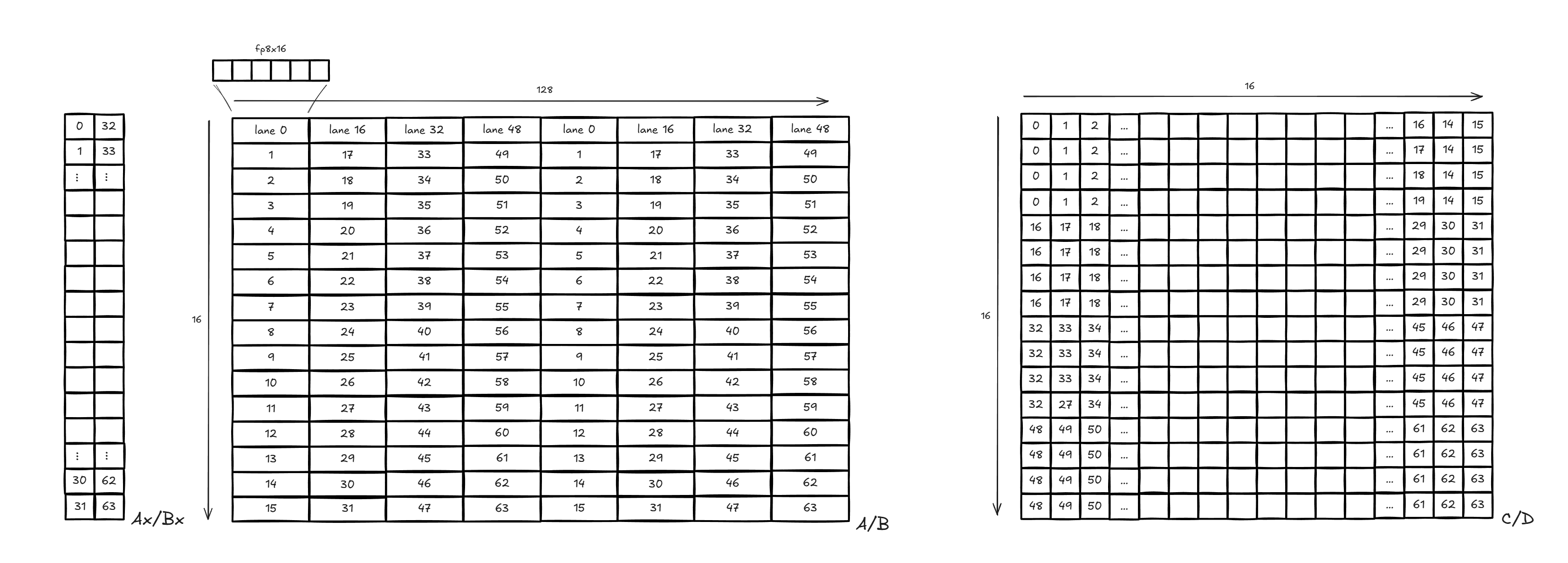
Figure 3: MFMA data layout#
To load A/B from LDS into registers, we use the ds_read_b128 instruction. This instruction allows us to load 128 consecutive bits (16 FP8 values) per thread.
Since we need a 16x128 fragment of A/B for each MFMA we’ll have to issue two ds_read_b128 per thread in order to load one fragment: (16*128) / (16*64) = 2.
The ds_read_b128 instruction is carried out in 4 phases, during which only a subset of threads is active. For the instruction to be bank conflict-free, all these phases must be conflict-free.
Unfortunately, the way we currently access A/B isn’t conflict-free as shown in figure 4.
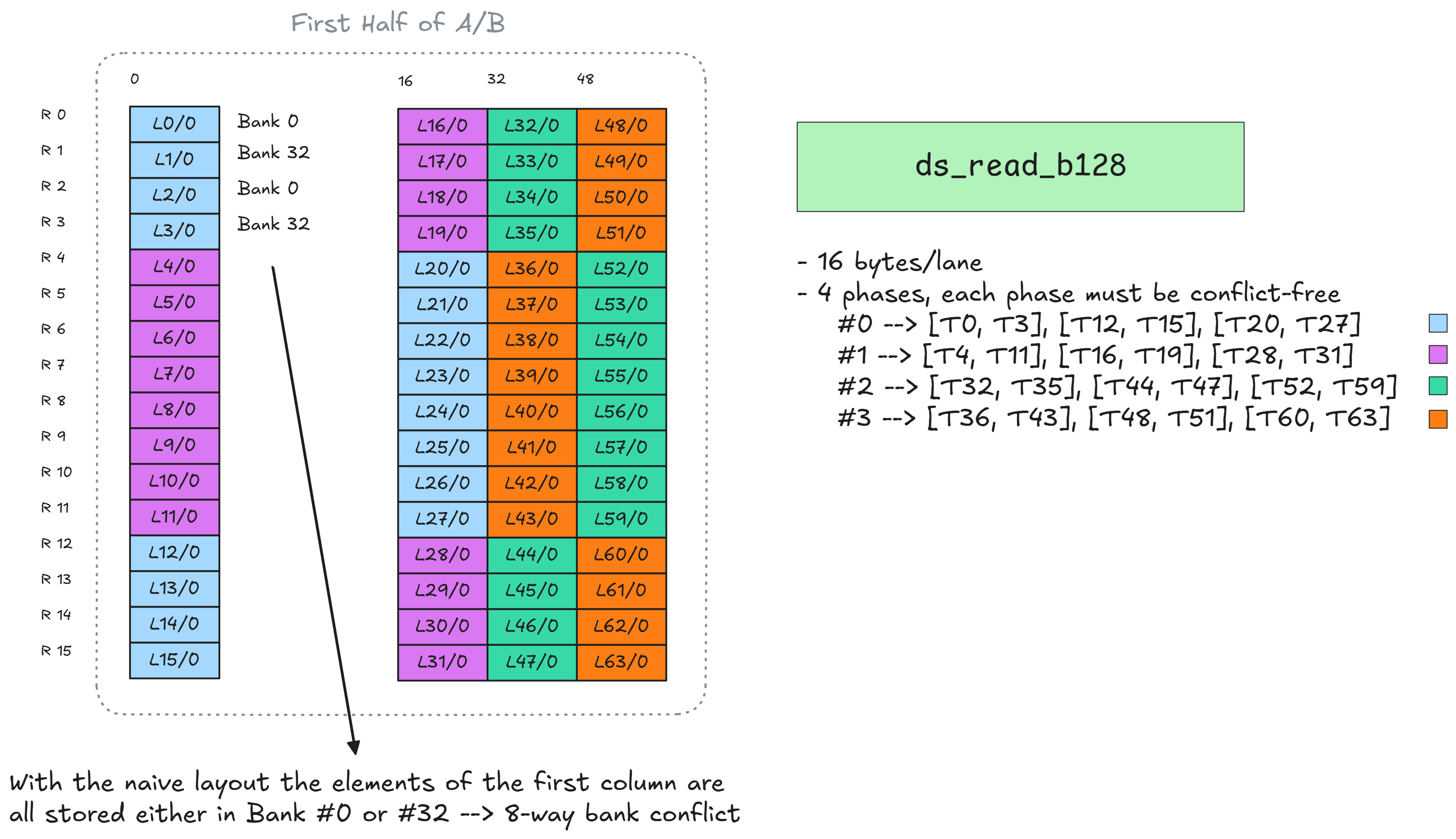
Figure 4: Bank conflicts in LDS access#
Each lane needs to access elements by column, but since the stride is 128 bytes, lanes along the same column will always hit the same two banks. This results in an 8-way bank conflict.
To eliminate bank conflicts, we need to change the way in which threads access data in LDS. We can achieve this by applying this swizzle pattern:
int2 swizzle(int row, int col) {
    int offset = row * 128 + col;
    // We need 11 bits for the offset:
    //  - offset[6:0] for the column
    //  - offset[10:7] for the row
    // To apply the swizzle just extract the row bits and XOR them with the column bits of the offset
    // We can tolerate two adjacent lanes to access elements in the same column so that's why we'll divide by 2
    int row_bits = (offset % (16 * 128) >> 7) / 2; // (or simply right-shift by 8)
    // bits[3:0] are always 0 because we access 16 bytes at a time
    int mask = row_bits << 4;
    int swizzled_offset = offset ^ mask;
    return {swizzled_offset / 128, swizzled_offset % 128};
}
Figure 5 shows how swizzling changes the access pattern. As you can see, we are now bank conflict-free during all four phases of the ds_read_b128 instruction.
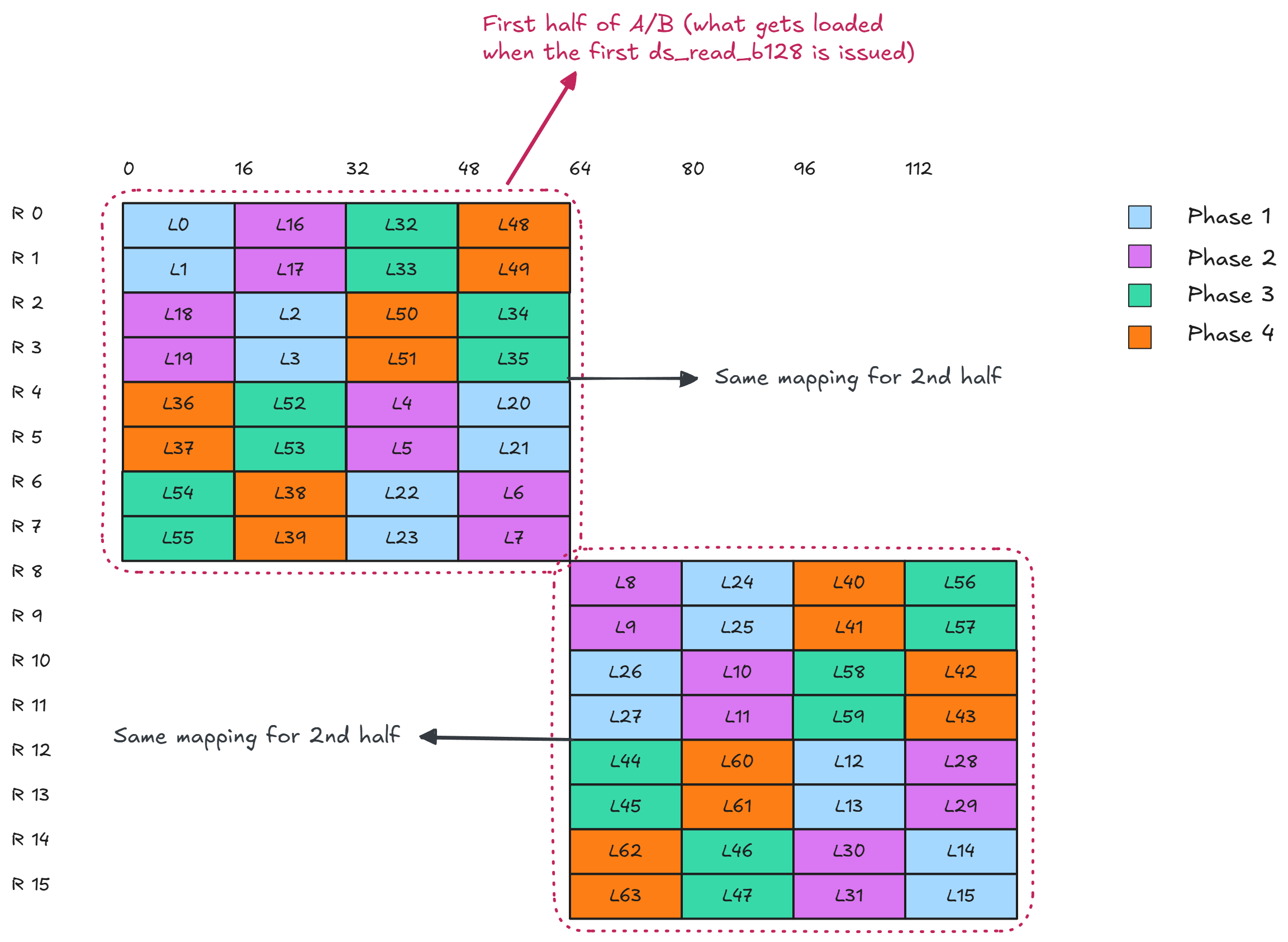
Figure 5: LDS swizzle#
Together with LDS swizzling, we’ll also apply a “chiplet-aware” swizzle in order to better optimize cache hit rates. The algorithm is detailed in Appendix A: Optimizing Cache Reuse. The idea is that we can change the way we compute the indices block_m and block_n shown in figure 2 by using some insights about the hardware to better utilize the cache hierarchy of our GPU.
Results#
Note
All tests were conducted on AMD Instinct™ MI355X GPU using ROCm 7.2.2. The workload is FP8 GEMM with BF16 output and FP32 accumulation.
Figure 6 shows a performance comparison of the two algorithms. For benchmarking, we used 1000 warm-up iterations, 1000 benchmark iterations, and rotating buffers along with normally distributed data. We report the average FLOP/s over 1000 benchmark iterations.
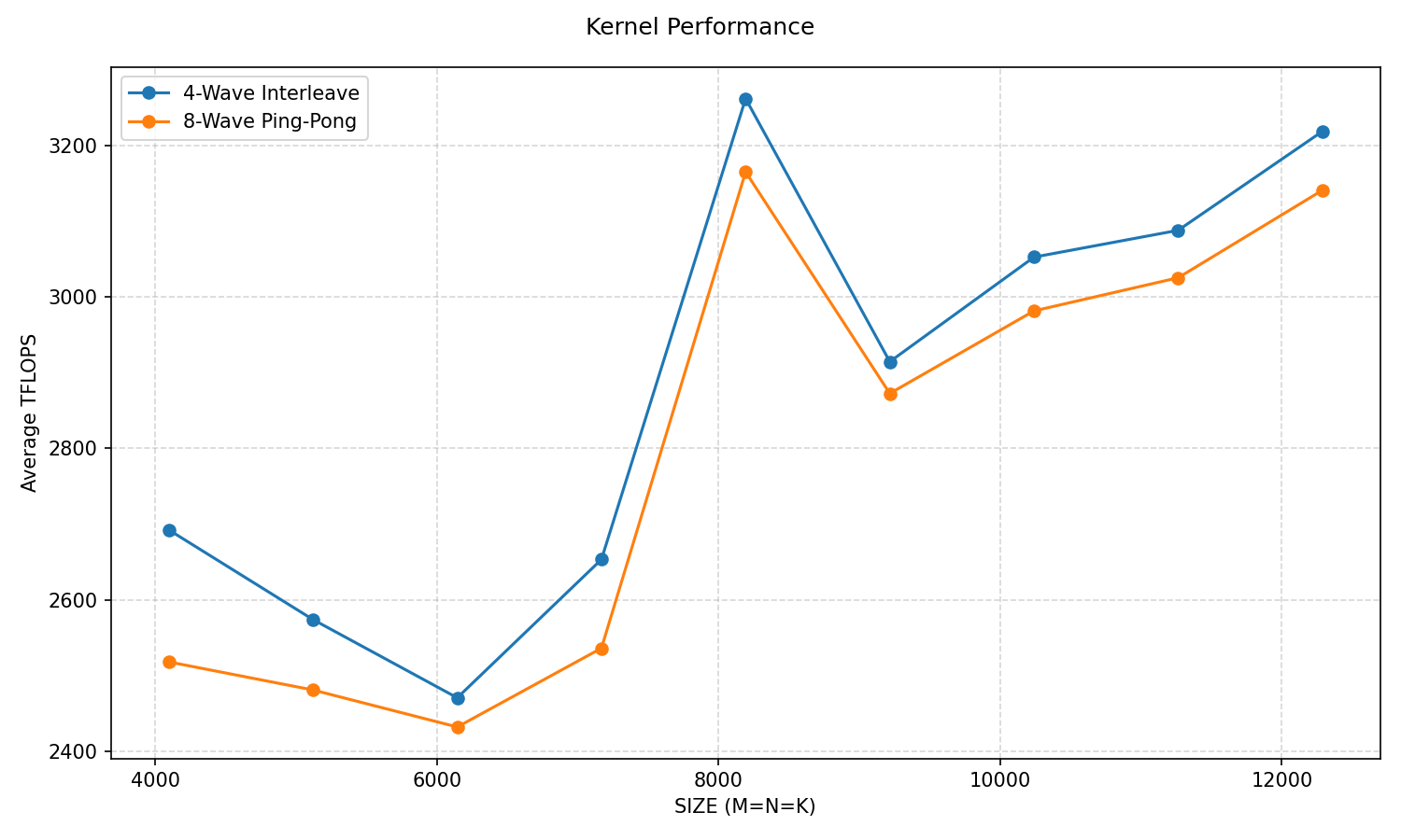
Figure 6: Performance comparison#
Summary#
In this blog, we presented the 4-wave interleave pattern from the HipKittens paper and explained how it differs architecturally from the 8-wave ping-pong design:
One wave per SIMD gives each wave the full 512-VGPR budget, enabling a larger 128×128 output register tile instead of 64×128.
Fine-grained software pipelining via
__builtin_amdgcn_sched_barrierinterleaves MFMA instructions with global→LDS and LDS→register loads at the sub-tile level, hiding memory latency without relying on the hardware scheduler to overlap two waves.Early accumulator store — storing completed
c[i][j]sub-tiles as soon as they are available rather than waiting for the full fragment — yields measurable performance gains across all test cases.LDS swizzling eliminates 8-way bank conflicts that arise from the column-major access pattern required by the
16×16×128MFMA instruction.Chiplet-aware grid swizzling (Appendix A) remaps thread block IDs so each XCD works on a compact rectangular region of the output matrix, maximizing both L2 and LLC hit rates on the MI355X’s 8-XCD topology.
The 4-wave design also proved more robust across compiler versions: unlike the 8-wave kernel, it required no manual #pragma unroll tuning to avoid register spilling and delivered consistent performance across different ROCm releases.
In an upcoming post, we will show how all of the above — the software pipeline, LDS swizzling, and grid scheduling — can be expressed concisely in FlyDSL, a Python DSL that generates high-performance HIP kernels while hiding much of the low-level scheduling complexity.
Further Reading#
For additional background and related work, see:
Configuration Details#
Data measured by AMD by the authors on May 11th, 2026. All the experiments were conducted on the AMD Instinct™ MI355X platform. System configuration:
GPU: MI355X-DLC 1.4KW
CPU: AMD EPYC 9575F 64-Core Processor
ROCm Version: 7.2.2
OS: Linux (Ubuntu 22.04)
Appendix A: Optimizing Cache Reuse#
In addition to the two schedules we discussed in this article, the HipKittens paper also introduced an algorithm to improve cache reuse on modern GPUs.
The key insight is that modern GPUs are moving towards a chiplet architecture rather than a monolithic one. For example, the AMD Instinct™ MI355X is a cluster of 8 chiplets called accelerated complex die, or XCD, each one with 32 compute units. Each XCD has an L2 cache and shares a Last Level Cache with the others. Ideally, we’d like to optimize for both cache levels:
Make thread blocks assigned to the same XCD reuse the same rows of A and the same columns of B as much as possible to optimize for the L2 cache.
Make multiple XCDs work on common regions of the input matrices so that shared data stays in the LLC as much as possible.
Consider the case where the number of XCDs is 3. With the naive grid schedule, tiles are assigned to XCDs in round-robin order as shown in the figure below:
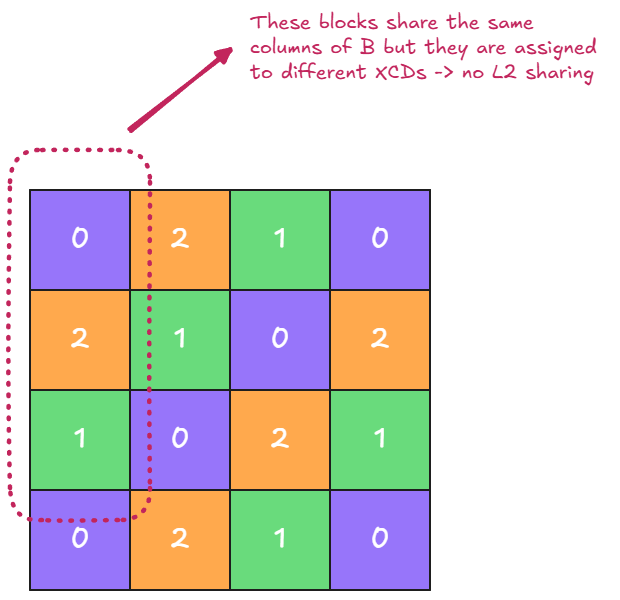
Figure 7: Naive Grid Schedule#
The HipKittens algorithm addresses this issue by remapping how tiles are assigned to thread blocks:
int remap_wgid(int wgid, int num_workgroups, int num_xcds, int chunk_size) {
    // Compute the XCD I'm currently on
    int xcd = wgid % num_xcds;

    // Each XCD gets chunk_size consecutive wgids
    int block = num_xcds * chunk_size;
    // How many full num_xcds * chunk_size blocks we have
    int limit = (num_workgroups / block) * block;

    if (wgid > limit) return wgid;

    // The order in which we are scheduled on this XCD
    int local = wgid / num_xcds;
    int chunk_idx = local / chunk_size;
    int offset_in_chunk = local % chunk_size;

    return chunk_idx * block + xcd * chunk_size + offset_in_chunk;
}

constexpr int NUM_XCDS = 8;
// WINDOW_SIZE and CHUNK_SIZE are constants that have to be tuned based on the hardware and the problem size
constexpr int WINDOW_SIZE = 4;
constexpr int CHUNK_SIZE = 8;

const int global_block_id = blockIdx.x;
int wgid = global_block_id;
const int num_workgroups = gridDim.x;

// Step 1: map CHUNK_SIZE consecutive wgid to the same XCD
wgid = remap_wgid(wgid, num_workgroups, NUM_XCDS, CHUNK_SIZE);

// Step 2: grouped tile assignment
const int num_m_blocks = ceil_div(M, BLOCK_M); // Number of blocks along M
const int num_n_blocks = ceil_div(N, BLOCK_N); // Number of blocks along N
const int num_wgid_in_group = WINDOW_SIZE * num_n_blocks;
const int group_id = wgid / num_wgid_in_group;
const int first_row = group_id * WINDOW_SIZE; // Each group spans WINDOW_SIZE rows
const int group_size_m = min(num_m_blocks - first_row, WINDOW_SIZE); // Handle edge case (partial group)
const int pos_within_group = wgid % num_wgid_in_group;
// Compute this tile row/column
const int block_m = first_row + (pos_within_group % group_size_m); // Advance in column-major order
const int block_n = pos_within_group / group_size_m;
At the end, each XCD will own a WINDOW_SIZE x CHUNK_SIZE / WINDOW_SIZE contiguous tile block.
If we take the same matrix as in figure 7 and apply this formula with WINDOW_SIZE=2 and CHUNK_SIZE=4 we get:
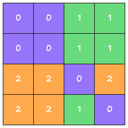
Figure 8: Grid Schedule with Swizzling#
By assigning a rectangular region of the output matrix to each XCD and assigning contiguous regions to contiguous XCDs, we can maximize both the L2 and LLC hit rates.
It’s worth pointing out that this algorithm requires hand-tuning in order to find the best schedule for a given GPU. The parameters
WINDOW_SIZE and CHUNK_SIZE must be tuned based on the hardware characteristics of your target GPU as well as the specific problem
size you wish to optimize for.
Disclaimers#
Third-party content is licensed to you directly by the third party that owns the content and is not licensed to you by AMD. ALL LINKED THIRD-PARTY CONTENT IS PROVIDED “AS IS” WITHOUT A WARRANTY OF ANY KIND. USE OF SUCH THIRD-PARTY CONTENT IS DONE AT YOUR SOLE DISCRETION AND UNDER NO CIRCUMSTANCES WILL AMD BE LIABLE TO YOU FOR ANY THIRD-PARTY CONTENT. YOU ASSUME ALL RISK AND ARE SOLELY RESPONSIBLE FOR ANY DAMAGES THAT MAY ARISE FROM YOUR USE OF THIRD-PARTY CONTENT.